From Electronics to Spintronics… and Now, Orbitronics?!
The history of information technology is deeply tied to how we manipulate one of the fundamental parts of the atom: the electron. Early on, engineers learned to move the electron’s negative charge through materials, which was used to create electrical currents and store energy through charge accumulation. This control over electrons became the foundation of most devices we use today. (Here, “electronics” comes from “electron,” and “electrical current” means electrons moving together.)
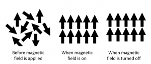
Later, exploiting another property of electrons — their spin — led to new advances. (For a deeper dive into the history and details of spintronics, see Mayank’s excellent post.) The spin of electrons is a complex concept. Still, macroscopically, it can be thought of as an intrinsic identity of the electron, like a color (red or blue) or an arrow (up or down). It gives rise to a tiny magnetic field per electron. By learning to control the spin, we opened the door to a new field called spintronics, where devices manipulate spin currents (electrons with a particular spin moving together) and spin accumulation (electrons with a specific spin gathering in one place).
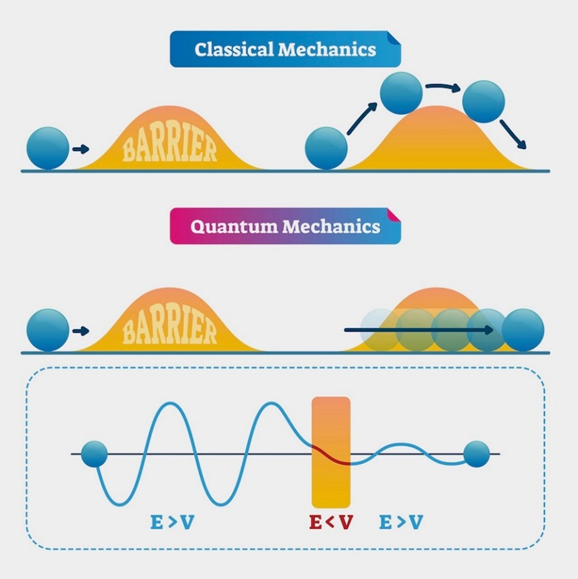
Of course, this is only a small part of the whole story. The spin is not the only property we can exploit. From the fundamentals of quantum mechanics, we know that an electron’s total angular momentum combines spin and orbital angular momentum — the latter arising from the complex, cloud-like paths that electrons trace as they move along the system and around the centers of atoms. These orbital motions create an additional magnetic moment, meaning electrons can carry magnetism from their spin and orbital motion.” This leads us to a second new set of names: orbitronics, orbital currents, and orbital accumulation.
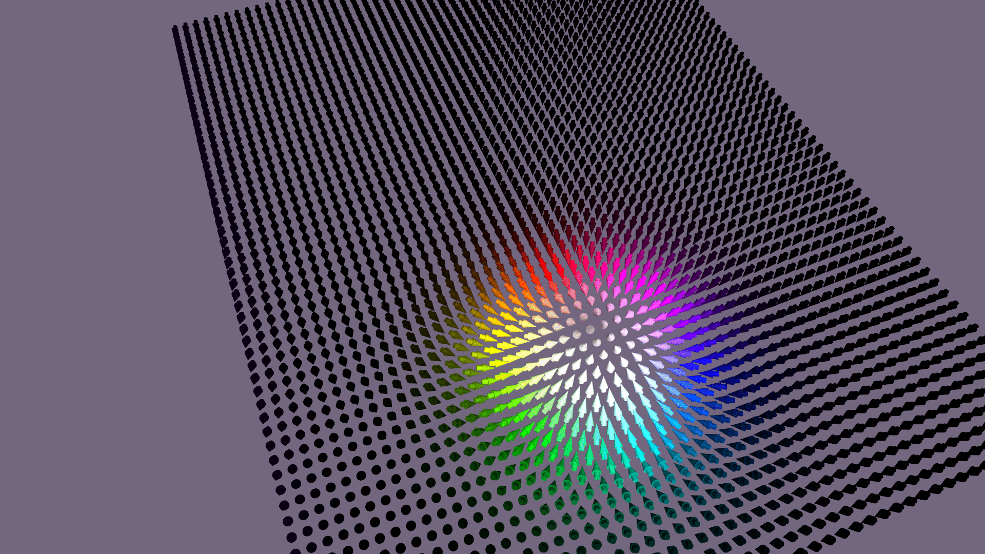
We can imagine an orbital current as a collective movement of electrons that rotate similarly as they move through a crystal (see the video above). However, detecting orbital accumulation — where orbital angular momentum builds up at material edges — is not as straightforward. It remains a topic of active discussion within the scientific community. For instance, during the recent SPEAR conference (Spin and Orbit in San Sebastián), leading researchers gathered to discuss the state of the art in orbitronics and the major experimental and theoretical challenges ahead.
If spintronics opens the door to new ways of using electrons, then orbitronics opens an additional window to even greater possibilities. Spintronics and orbitronics are deeply intertwined, so separating the effects of spin and orbital currents in many experiments is exceptionally challenging.
This is where my own research comes in.
I study charge-to-spin and orbital conversion — how an incoming electrical current can be transformed into spin and orbital currents. They have to be produced somehow by answering key questions — how, why, how much, and under what conditions — we can identify promising materials that maximize useful effects while minimizing cost and complexity.
Physics is endlessly fascinating on its own, but at some point, our work must also aim toward practical goals: making future devices faster, cheaper, more energy-efficient, and more environmentally friendly.
Despite the current uncertainties, the future of orbitronics is bright. Mastering the orbital degree of freedom is part of a much larger trend: learning to control the hidden properties of electrons and materials.
Under the growing umbrella of “X-Tronics,” fields like: – Valleytronics (controlling electrons based on energy valleys), – Twistronics (tuning properties by twisting atomic layers), – Phononics (managing atomic vibrations),
are rapidly expanding.
The next technological revolution might not be about moving more electrons — but about moving them smarter and more efficiently.
Have you ever wondered how your brain effortlessly recognizes faces, understands language, makes quick decisions, or learns from past experiences? These seemingly simple tasks pose significant challenges for conventional computers, which consume considerable energy handling precise numerical calculations step-by-step. The brain’s remarkable efficiency arises from its ability to perform numerous parallel computations simultaneously, often with lower precision. This observation raises an intriguing question: Can artificial systems replicate the brain’s impressive efficiency?
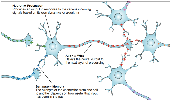
Neuromorphic computing tackles exactly this challenge. This emerging technology aims to mimic the brain’s structure and function, specifically its essential components—neurons and synapses. Neurons are tiny processing units interconnected by synapses that transmit electrical signals known as spikes. Remarkably, the human brain accomplishes all these tasks while consuming only about 20 watts of energy—comparable to a dim light bulb—demonstrating exceptional efficiency. By replicating these biological interactions, neuromorphic computing promises substantial improvements in computational power and energy efficiency, potentially leading to powerful yet sustainable solutions.
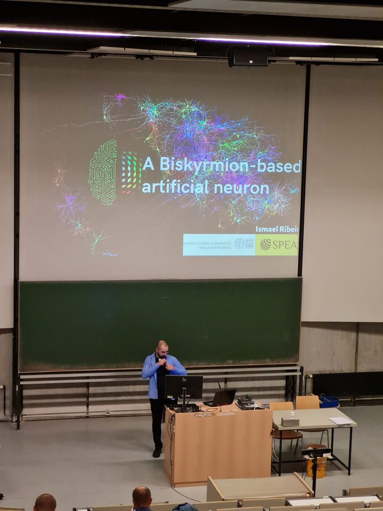
One promising technology for neuromorphic computing is spintronics, which utilizes the magnetic spins of electrons to build innovative devices. There are several ways to use spintronic devices for neuromorphic computing. I will talk about my favorite: magnetic skyrmions! Imagine a skyrmion as a tiny magnetic vortex, where electron spins align into stable, swirling patterns resembling miniature whirlpools or galaxies, but in a magnetic material. This intricate configuration gives skyrmions remarkable stability, allowing them to be reliably manipulated by electrical currents at nanoscale dimensions (see figure for a visual example).
Biological neurons can be effectively modeled using RC circuits—basic electronic components combining resistance (R) and capacitance (C) to control electrical signals. These circuits capture the essential dynamics of neurons through the Leaky-Integrate-Fire (LIF) model, which is widely adopted in neuroscience to describe neuron behavior. Remarkably, skyrmions can replicate these neuronal dynamics at a nanoscale. By placing a skyrmion within a specially engineered magnetic environment where the perpendicular magnetic anisotropy (PMA)—which defines how strongly spins prefer aligning perpendicular to the surface—varies quadratically, the skyrmion moves predictably under electrical stimulation. The applied current induces a force that competes with the force due to the gradient, causing the skyrmion to shift its position, similar to how voltage accumulates in a capacitor during charging. Once the current ceases, the skyrmion naturally returns to its original position, effectively simulating the discharge phase of a capacitor. This motion directly mirrors the LIF neuron’s behavior, which shows that skyrmions have the potential to efficiently emulate biological neuron dynamics.
Scaling these skyrmion-based neuromorphic devices involves overcoming challenges in precise fabrication, maintaining stability, and integrating them into existing technologies. Despite these challenges, skyrmions might have a crucial role in neuromorphic computing. So, can we emulate the brain? Well, at least NOT YET :((. However, scientists have been able to emulate individual neurons with skyrmions (and other spintronic devices). Given that the brain consists of billions upon billions of interconnected neurons, I guess we could say, “Let’s take one neuron at a time… one neuron at a time.”
Van der Waals Heterostructures: From Bulk Crystals to Devices
Materials science has made leaps in recent decades, particularly with the discovery and manipulation of two-dimensional (2D) materials—ultrathin sheets of atoms with unique electronic and magnetic properties. Everything began with the discovery of graphene in 2004, a single layer of carbon atoms with exceptional electrical and mechanical properties. Researchers in Manchester were able to separate a single layer of carbon from its bulk crystal using household sticky tape.
Building on this discovery, researchers began exploring other 2D materials, broadening the possibilities of material science. In the beginning, only a handful of materials were known and used for research. In addition to metallic graphene and insulating hexagonal boron nitride (hBN), more and more materials have been discovered, including magnetic materials, semimetals, and superconductors.
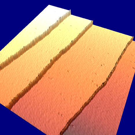
By stacking different 2D materials on top of each other, scientists can create van der Waals heterostructures. These engineered materials offer unprecedented control over electronic and optical properties, leading to significant advancements in electronics, quantum computing, and spintronics., named after the weak interlayer forces that hold them together. These structures allow researchers to tailor new materials with properties that do not exist in nature, leading to advancements in electronics, quantum computing, and spintronics. While the initial methods for creating artificial crystals were highly complex and had limited success, this changed with the introduction of the PDMS-PC dry stacking technique. A device that was created using this technique is shown in Fig. 1. The bulk material images were taken from the website of the Quantum Materials Lab of the University of Arkansas which provides a great overview of exfoliatable materials.
Fig. 1 Comparison of bulk crystals and artificial heterostructures created from exfoliated flakes of these materials.
Before constructing these heterostructures, researchers must first prepare the thin crystal sheets. Using adhesive tape, thin flakes of layered crystal are peeled from a bulk crystal. Basically, the thickness of the crystal pieces is halved with every iteration of opening and closing a piece of tape. Instead of the household scotch tape, researchers nowadays employ blue tape. This tape type of tape is usually used to cover example items to protect their surfaces and is used by researchers due to its low adhesive residues. The process is shown in Fig. 2. These flakes are then transferred on silicon wafers and inspected under an optical microscope to identify those with the right thickness and quality.
Fig. 2a) Natural graphite flakes, and b), c) successive stages of the exfoliation process, illustrating the gradual reduction in thickness as layers are further separated.
With the selected flakes in hand, researchers use the PDMS (polydimethylsiloxane)/PC (polycarbonate) Dry Transfer method to assemble artificial crystals layer by layer, ensuring precision and purity. As illustrated in Fig. 3, this process involves several key steps that allow for high control over layer alignment and minimal contamination.
Fig. 3 Step-by-step process of the dry transfer method using PDMS and PC: a) The PDMS-PC stamp is aligned over a selected flake. b) The flake is picked up by gently pressing the stamp while applying heat. c) The lifted flake is ready for stacking, and this process can be repeated to layer multiple flakes – usually, only the first flake requires heat. d) The stack is transferred to a different substrate. e) The flake is carefully aligned with pre-patterned electrical contacts and deposited at temperatures above 160°C. f) The PC layer is dissolved in chloroform, leaving a clean, high-quality van der Waals stack.
A PDMS stamp coated with a thin layer of PC is used to pick up an exfoliated 2D material. This stamp is then aligned over the target substrate under a microscope. By carefully controlling the temperature and pressure, the material is released onto the stack without contamination. The polycarbonate layer is later dissolved, leaving a clean heterostructure. This dry transfer method provides a high level of control over layer alignment and minimizes impurities, making it an essential tool for studying and engineering advanced 2D material-based devices. Following, the steps are described in more detail:
Flake Selection and Alignment: A PDMS stamp coated with a thin layer of PC is first aligned over a selected 2D material flake using a microscope. This step ensures precise positioning of the flake for pickup.
Flake Pickup: The stamp is gently pressed onto the flake while applying mild heat. This softens the PC layer, allowing the flake to adhere to it. Once lifted, the flake is securely attached to the stamp.
Stacking Multiple Layers: The pickup process can be repeated to stack multiple flakes on top of each other. Typically, only the first flake requires heat; subsequent flakes attach through van der Waals forces alone.
Substrate Transfer: After assembling the desired stack, the PDMS-PC stamp is moved to a different substrate, such as a silicon wafer or a pre-patterned chip with electrical contacts.
Final Alignment and Deposition: The flake is carefully positioned over pre-fabricated electrical contacts and deposited at temperatures above 160°C, which ensures good adhesion and minimizes contamination.
Polycarbonate Removal:The PC layer is dissolved using chloroform, leaving behind a clean, high-quality van der Waals heterostructure, ready for further experiments or device fabrication.
Ultimately, van der Waals heterostructures serve as a foundation for next-generation nanotechnology, enabling innovations in data storage, high-speed electronics, and beyond. From spintronic devices that store information using electron spin to high-speed, ultra-efficient transistors, these materials push the boundaries of what is possible. By refining fabrication techniques, researchers can fine-tune these structures to develop new quantum materials, flexible electronics, and energy-efficient computing devices. As our ability to design and manipulate materials at the atomic level continues to improve, van der Waals heterostructures will remain at the forefront of scientific and technological breakthroughs.
I had in mind writing a very happy and cheerful post based on the last few trips and successes in the research. However, as I read the previous post to feel the vibe of the blog, I realized that the last few are related to “the last blog post.” It took me a while to accept that the end has become more real than ever. I have never been good at goodbyes; somehow, it always feels like I didn’t say enough, while at the same time, I said too much and couldn’t enjoy the last words and silence. So, I’ve decided to start with that and deal with the regret later.
Thanks to everyone in SPEAR, every speaker, every training organizer, and every person I met during the secondments. Thanks to the PIs, thanks to Ingrid and Annika, thanks to Ismael and the group in Halle, and thanks to every ESR; I will always remember you and miss you all!! And to the one who made the project work, Eli, thank you very much!
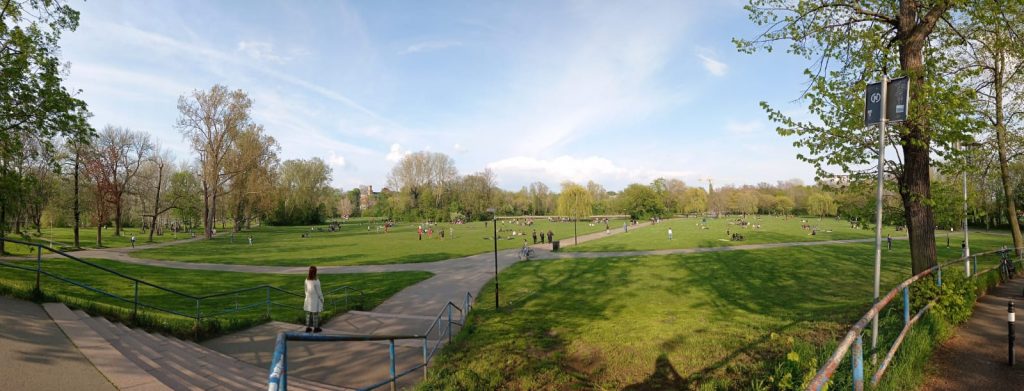
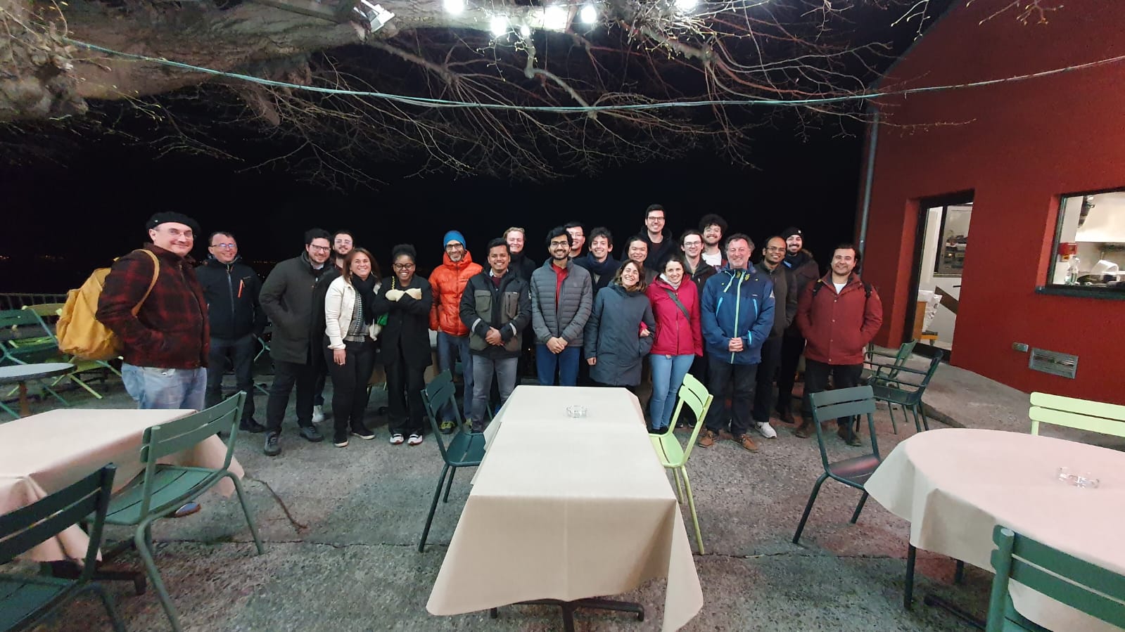
Bad Honnef Workshop January 2023.
Bad Honnef Workshop January 2024.
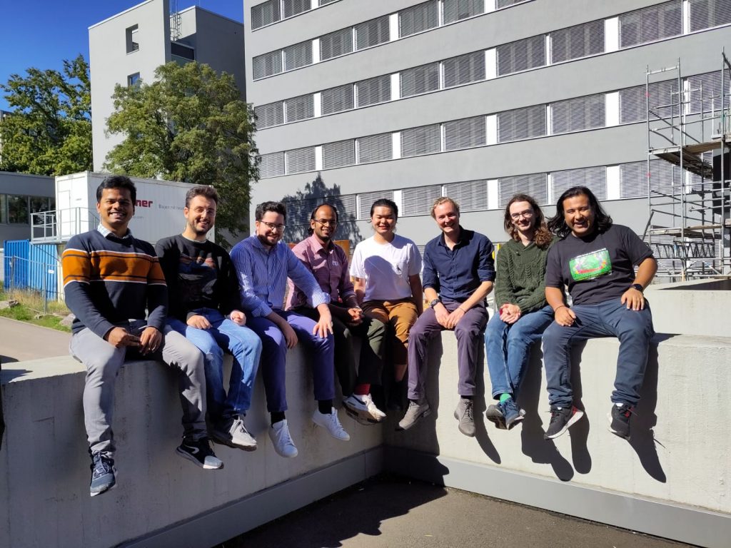
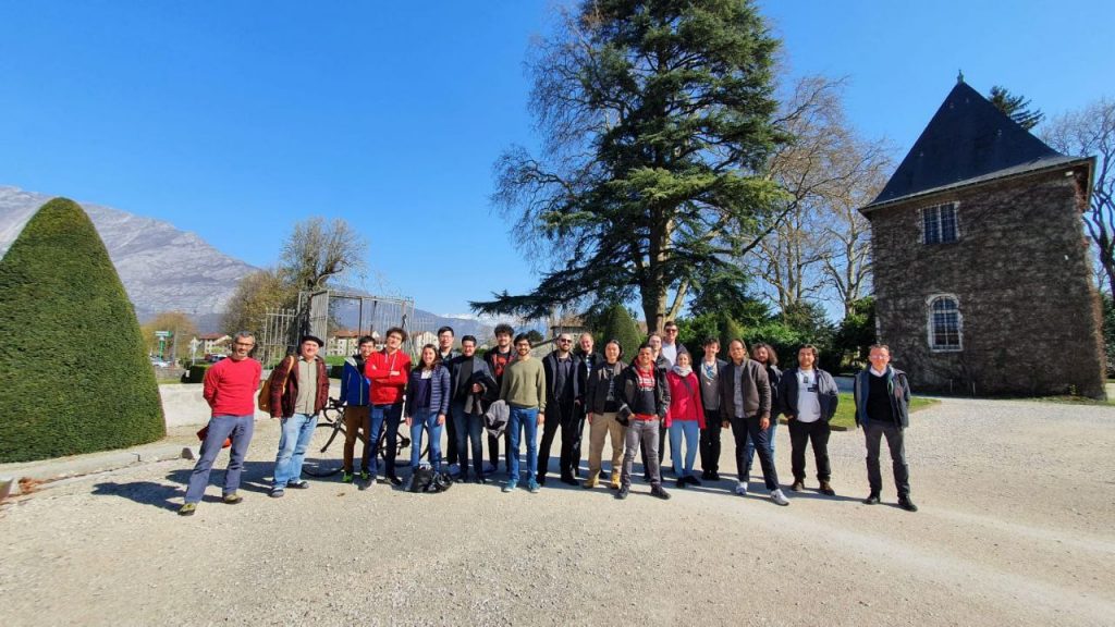
Now that the PhD time is coming to an end, more and more goodbyes are coming. Either because some people already left or because I might be going somewhere else. Before Christmas, I had what could be “the last group photo” with the first group of friends I made during the PhD. It was mixed with joy from seeing them and sadness since we might not be together anymore. Time definitely runs faster when you have fun!. Luckily, we immortalized the moment with an instant photo for each one so that we were together even with countries in between.
One thing I know for sure is that it has been a crazy ride. Whenever I start telling the stories I got from the PhD, it always feels impossible or made up. Stories of conferences in crazy places, of the knee surgery, of the parties, of going from a struggle to the celebrations, it does not make sense that everything happened in 3 years. How is it possible to have so much fun, meet so many amazing people, and experience so much of the world in just three years? Three!! This must be some kind of magic.
Anyhow, we have at least one more goodbye, and for once, I am really looking forward to meeting again in San Sebastian!. Prost to SPEAR, Halle, and all of you.
Last week, I had the privilege of attending the 2025 MMM-Intermag Conference in New Orleans alongside my colleague Simon. This event, centered on cutting-edge research in magnetism, provided an excellent platform to introduce QZabre and our nitrogen vacancy (NV) technologyto the broader magnetism community.
Our primary role at the conference was to represent QZabre at our booth in the exhibition hall. Unlike simply attending talks or poster sessions, this hands-on engagement offered a unique perspective. Interacting with a diverse range of attendees—including scientists, engineers, and industry professionals—was a particularly enriching experience. Each visitor brought their own perspectives and challenges, sparking dynamic conversations.
While our primary focus was on scanning nitrogen vacancy magnetometry (SNVM), the questions and discussions extended well beyond that. Some attendees were curious about quantum sensing and its potential, while others explored how SNVM could enhance their research or how it could address industrial challenges. Engaging in these discussions and tailoring potential solutions to the needs of our visitors was incredibly fulfilling. Advocating for the versatility and power of SNVM and seeing its potential to make an impact reinforced the importance of the work we do.
The conference schedule was tight, as is typical for such exhibition events, but the experience was both rewarding. On the final night of our stay, we found a moment to explore New Orleans. Known for its vibrant culture and rich musical heritage, the city provided a memorable and enjoyable conclusion to our trip.
Wrapping Up and Recharging: A PhD Journey through the Holidays
The days before the Christmas holidays are usually hectic since many people want to wrap things up and start the new year fresh. This was the same for me too! I did my halfway seminar at the end of November. Here in Sweden, half-way seminars are intended for PhDs who have passed almost two years of their journey and is an evaluation to the progress they’ve made. To me, it was a very good opportunity to assess where I am and where I want/need to be in my academic career.
With that ending, I could enjoy New Year’s holidays peacefully since I decided to stay home and relax! Usually, holiday travels come with a lot of tiredness afterward (which requires another holiday on top!), and I needed some time to myself to keep distance from all the PhD work, and do nothing!
Now that life has regained its pace and we’re back to the routine again, I’m looking forward to starting new projects with energy, and of course, seeing our network at the final spear conference in San Sebastien!
Hello people and wish you a happy new year 2025! This will be my last blog of SPEAR as my PhD is coming to an end in a few months.
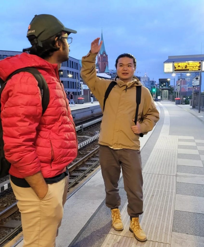
I just came back from Zurich where I visited my friend Zhewen, ESR 13 who lives in Zurich. We had a lot of fun touring a lot of places in Switzerland and besides being a very good researcher, Zhewen is also a great tourist guide!
This is me standing in the picteresque landscape city of Lauterbrunnen! Thanks to Mr. Zhewen Xu!
Reflecting back on the year, I am happy with how things have progressed in my PhD. There will always be ‘ifs’ and ‘buts’ wherever you go. But taking only the positives with me from my PhD experience, I am venturing into the last phase now, where I am currently writing my thesis and will defend in a few months from now. Hamburg has been a special place in my life, both academically and personally. I went through many highs and lows which shaped me into a better individual.
The SPEAR program has proven to be challenging with respect to the time in one’s PhD. But these kind of challenges made me to learn adaption even better. I started my PhD with no experience in the technique I use now, i.e. STM and now I value this technique very much. I plan to stay in academia and stay loyal to STM and it’s different variants 🙂
I am looking forward with excitement to the wrapping up SPEAR conference to be held in San Sebastian, Spain in April! These coming months until the SPEAR conference will be busy and intense for me. But I enjoy intense situations as I perform better under pressure xD. I wish all my co-ESRs a happy remainder of their PhD and congratulations to Salvatore (ESR 7) for finishing his PhD successfully! Thank you everyone for your warm friendship and wish you all a nice year ahead 🙂
It all makes me wonder whether anyone has been reading along with me, refreshing the page, anxiously anticipating the next installment, or if I’ve been screaming into the void this entire time?
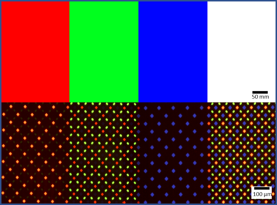
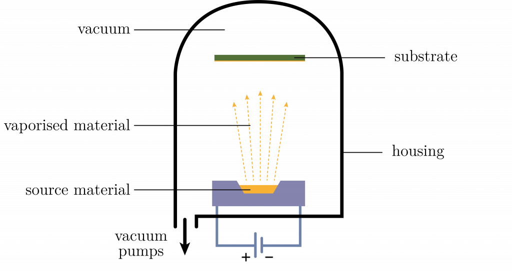
Making graphene is a critical part of any graphene based project, like mine. But how do we make it? Actually its much easier than one might expect – during lab outreach events we’ve had children with no training whatsoever make perfectly presentable pieces, a fact that really calls into question the value of my two master’s degrees.
The first step in creating graphene involves using scientific-grade adhesive tape to peel a thin layer from a larger piece of graphite, a material composed entirely of carbon atoms arranged in a layered structure. Graphite is similar to the “lead” found in pencils, but in this process, we are interested in isolating its single-layer form, known as graphene. The tape serves as a tool to cleave the graphite, capturing the topmost layers.
Next, the adhesive side of the tape, now holding thin graphite flakes, is pressed firmly onto a meticulously cleaned silicon wafer. Silicon is chosen because its properties enhance graphene visibility under certain lighting conditions, as well as being a convenient surface to do further work on the graphene. The wafer is then heated to improve adhesion, ensuring that some graphite flakes stick properly to its surface. After allowing sufficient time for this process, the tape is slowly and carefully peeled away. This peeling leaves behind an uneven distribution of graphene flakes on the silicon wafer, with pieces varying in size and thickness.
To locate a suitable piece of graphene, we turn to an optical microscope. This instrument allows us to inspect the wafer’s surface with precision. Graphene interacts uniquely with visible light, absorbing it efficiently, which causes it to appear darker than the surrounding silicon. This optical contrast makes it possible to differentiate between flakes of varying thickness. By observing how dark each flake looks, we can estimate the number of graphene layers present, ultimately selecting the desired single-layer graphene for further experimentation.
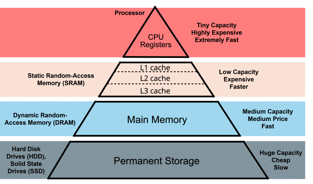
Towards a high density and low power magnetoresistive random-access memory (MRAM)
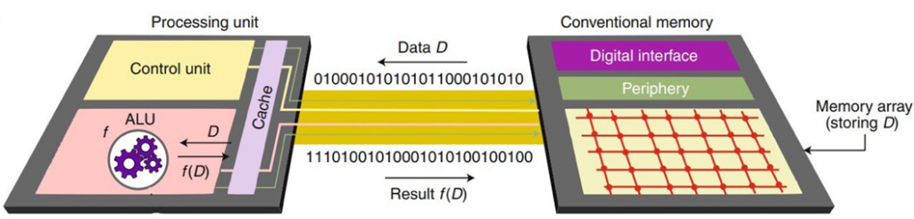
Memory matters! First, let’s look at the definition of computer memory from Wikipedia, ‘memory is a device or system that is used to store information for immediate use in a computer or related computer hardware and digital electronic devices 1.’ Based on Von Neumann’s architecture, a memory can store many data coded in binary, which are ‘0’ and ‘1’. All information is stored and processed in the form of binary bits. Thanks to memory, your smartphone or laptop can keep up with your endless selfies, streaming, and meme collection. These days, we demand so much from our devices that the memory inside has to work faster, be more efficient, and somehow use less power. Our iPhones or Androids are crammed with memory chips that now go up to gigabytes or even terabytes, yet our hunger for more memory never seems to be satisfied. Plus, our devices run out of battery way too fast! The MRAM is a magical-sounding memory tech that could solve our tech troubles.
Figure 1. The schematic of binary bits in MRAM
What is MRAM? Magnetoresistive random-access memory (MRAM) is a promising candidate for next-generation memory, as it is a non-volatile (it doesn’t lose data when powered off), fast-speed, high-density, and energy-efficient memory technology. Figure 1 shows the core of a MRAM cell, magnetic tunnel junction which is a pillar consisting of three layers. They include two ferromagnetic layers separated by one spacer. The magnetization directions of top and bottom ferromagnets are pointed out by arrows. In Figure 1, the magnetization of top layer is fixed, while the bottom free layer’s magnetization can be switched by an external magnetic field or current.
Figure 2. The schematic of STT-MRAM (left) and SOT-MRAM (right).
How does MRAM work? There are a few tricks to this in MRAM. Early MRAM used external magnetic fields to get the job done, but that required a lot of energy (and wasn’t too stable). Luckily, scientists came up with some new ways: spin-transfer torque (STT)2 and spin-orbit torque (SOT)3. In STT-MRAM, an electric current (green line) passes through the device directly to flip the free magnetic layer. In SOT-MRAM, there’s an extra path for this current, which uses something called the spin Hall effect (fancy physics term alert) to change the magnet direction. Separated write and read lines ensure excellent endurance and the switching time under SOT can be achieved in sub-ns. While these two methods have their differences, the way MRAM reads data is pretty much the same across the board. MRAM “reads” by measuring the resistance between the two magnetic layers. When the magnets are parallel, the resistance is low — that’s our “0.” When they’re anti-parallel, the resistance is high — a “1.”
Figure 3. Comparison between STT-MRAM and SOT-MRAM.
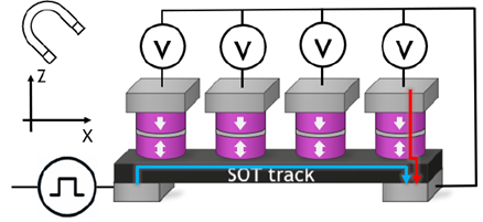
The future of MRAM — high density and low power From Figure 3, although the SOT-MRAM has a high endurance benefit from the separated path, it has three terminals resulting in a low integration density. A multi-pillar design was proposed to solve this problem (Figure 4)4. In conventional single-pillar devices, one pillar needs at least two transistors. In multi-pillar devices, the number of required transistors per pillar can be reduced to (1+1/N), where N is the number of pillars. The reduced number of transistors can effectively save space and improve the density of devices.
Figure 4. The schematic of a 4-pillar SOT-MRAM.
In principle, the multi-pillar device cannot work without the individual control of each pillar. Because all four pillars will be switched together when we only want to write on a specific cell, leading to a chaos of information. To solve this problem, applying a gate voltage can realize the selective operation in multi-pillar devices. To be specific, a positive gate voltage can lower the energy barrier between the ‘0’ state and ‘1’ state to decrease the critical switching current, while a negative voltage can increase it (Figure 5). On the one hand, during the selective operation, only the pillar under positive gates can be switched. By applying a specific gate voltage on each pillar, we can control which pillar will be written individually. On the other hand, the positive gate voltage can lead to a low working power.
Figure 5. The schematic of MRAM under gate voltage.
In short, MRAM is not only cool, but it could actually be a game changer for the future of electronics. So, next time you pick up your phone or use your smartwatch, think about all the tiny magnetic switches making it tick.
Ralph, Daniel C., and Mark D. Stiles. “Spin transfer torques.” Journal of Magnetism and Magnetic Materials 320.7 (2008): 1190-1216. ↩︎
Gambardella, Pietro, and Ioan Mihai Miron. “Current-induced spin–orbit torques.” Philosophical Transactions of the Royal Society A: Mathematical, Physical and Engineering Sciences 369.1948 (2011): 3175-3197. ↩︎
Cai, K., et al. “Selective operations of multi-pillar SOT-MRAM for high density and low power embedded memories.” 2022 IEEE Symposium on VLSI Technology and Circuits (VLSI Technology and Circuits). IEEE, 2022. ↩︎
Thanks for your reading. The story of MRAM is continuing. If you have questions, feel free to contact me at email: kaiquan.fan@imec.be
The summer has passed, and the leaves have turned orange; some have even started to fall. For me, this marks the end of my PhD’s (net)work.Since July, I’ve been on the move with business trips, conference presentations, and, of course, a bit of the usual summer vacation. It’s been a packed few months with a lot of great memories. I got to present my work, win an art contest at the ICM conference in Italy with the image below.
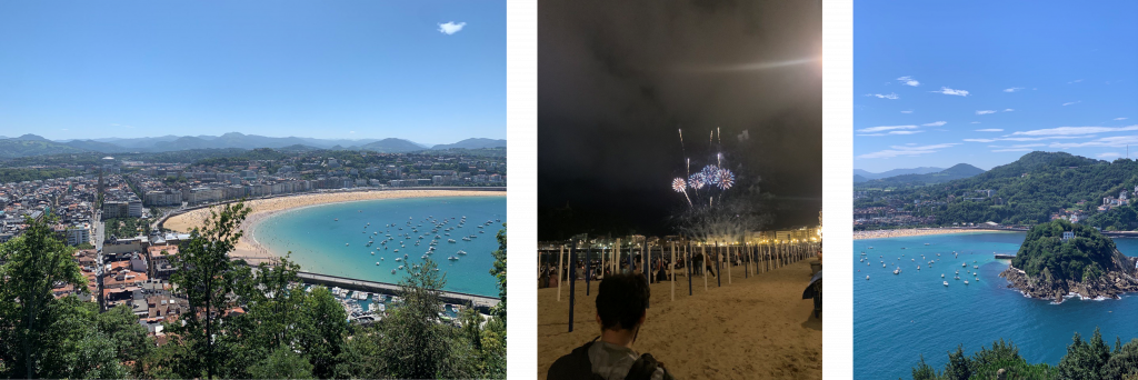
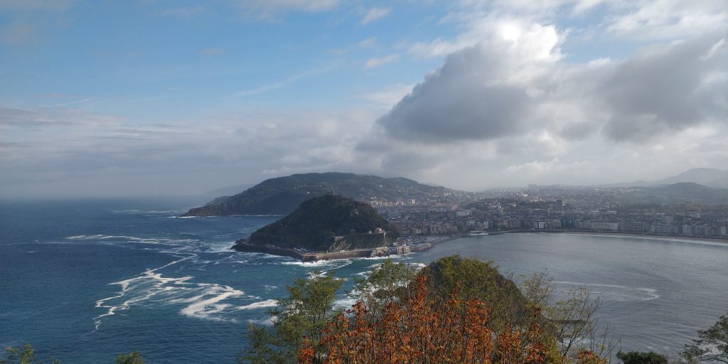
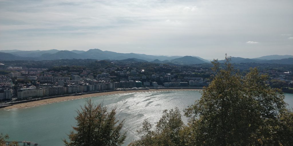
During my secondment, I spent time in the beautiful city of San Sebastián, where I enjoyed pintxos, the beach, and the beautiful hikes. In the middle of all this, I also organized a retreat for the International Max Planck Research School (IMPRS), which I am part of at the Max Planck Institute in Germany. Much of the inspiration for planning this retreat came from my experience at a summer school organized by ESR 3, Marco, back in 2022 in Lausanne, Switzerland. That summer school remains the best conference/school I’ve ever attended—it truly influenced my research interests and shaped the direction of my PhD. Below is a picture of one of the round tables from our retreat, inspired by the ones in Marco’s school. Here, I’m discussing creativity in science with Dr. Stuart Parkin (the mind behind racetrack memory, a core concept in my SPEAR project), Dr. Hyunsoo Yang, and Dr. Amir Capua.
In between all these trips, there was still plenty of work to do. I wrote my final PhD paper, which I’m currently in the process of submitting. This work has been a long time in the making and will be the core of my PhD thesis. With this final paper, I finally managed to bridge my research on skyrmions with neuroscience. It’s taken everything I’ve learned from my previous papers to understand the conditions that can make a skyrmion truly behave like an artificial neuron—something I’ve been pursuing for a long time.
Now, as I reach the end of my time with the SPEAR network project, I can’t help but feel like I’m closing one of the most meaningful and exciting chapters of my life. I have to give a special thanks to the person who helped make this project a success: our coordinator, Eli. Beyond her patience with my delayed reports (sorry, Eli!), she’s just an incredible person who has been a true pillar in this journey. I also want to thank Sofia for her role in our soft skills training. Her empathy and kindness in working with a bunch of skeptical physicists was something to admire, and I genuinely believe her guidance has made me a better presenter and scientist.
Finally, a big thank you to all the ESRs! It was a joy getting to know each of you, and I wish you all the best in your future endeavors. This project aimed to build a network of researchers, and I have to admit that I initially underestimated the power of networking in science. But looking back on my PhD journey, I can see the impact clearly. The connections and exchanges I was exposed to through the SPEAR project have shaped my research, my future, and who I am. Simply put, thank you all!
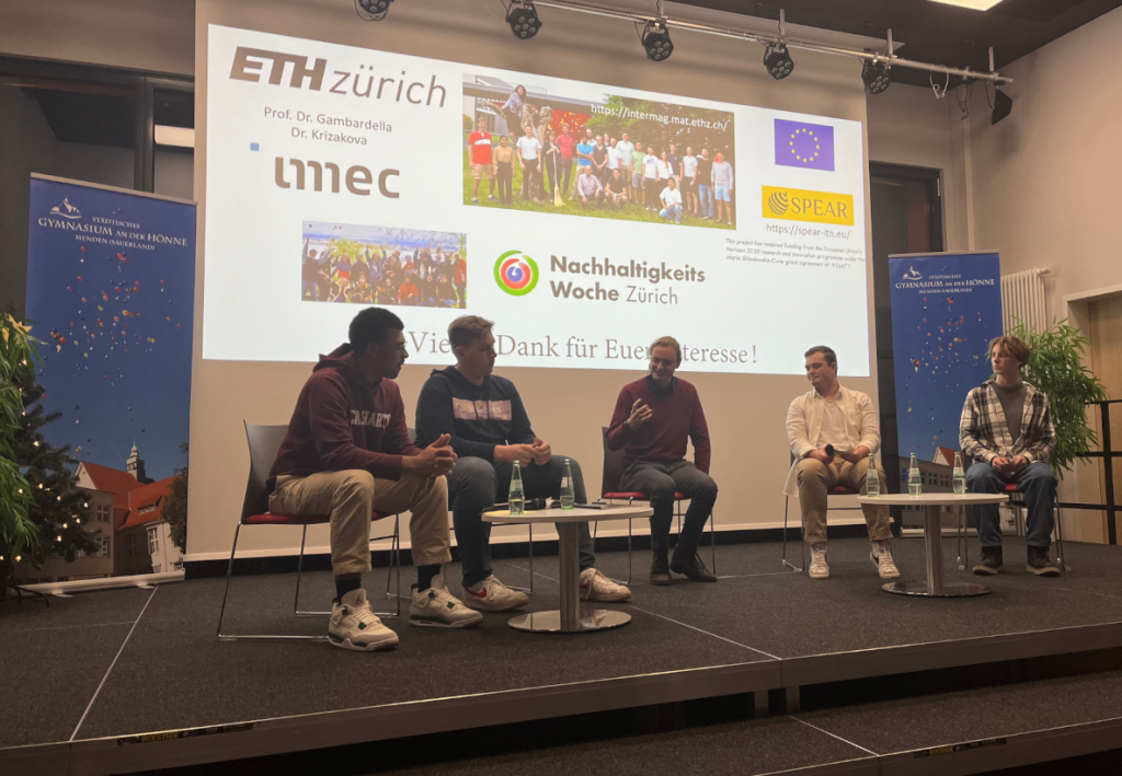
Discussing pathways towards a more sustainable future
Pursuing a PhD degree does not only mean to spend long hours in the lab trying to make tricky experiments work out and report on them. Educational institutions are not only places to study theoretical concepts and gain (scientific) experience. Thanks to the presence of professors and experts in diverse fields of study, close ties to politicians and industry as well as thousands of motivated students eager to learn, universities are also the ideal hub to connect all of these people to analyse, discuss and possibly tackle the problems our societies face in present and future. This enables everyone involved to learn from each other and grow together in the process.
Now you may wonder: “How can academic institutions function as such a hub and how does that look in detail?”
While there is a variety of good answer to the first questions, I will describe in the following one way that I have encountered, appreciated and grown a part of during the last three years: The sustainability week Zurich (https://nachhaltigkeitswoche.ch).
This is a student association supported by all five institutes of higher education in Zurich (ETHZ, University of Zurich, the teachers’ school, the university of applied sciences, and the art academy) but not associated to any political party. We are entirely run by students to organize a set of events targeting the topic of sustainability once a year and maintaining the interest via smaller educational and yet fun events throughout the year. Sustainability may originate from the long-term oriented industrial usage of forests to avoid over-exploitation and is often used as a concept to counteract climate crisis and mass extinction. However, nowadays it also entails social, political and psychological dimensions, thus exceeding beyond the classical scope of the protection of biotopes.
Considering the diversity of people and topics, a plethora of opportunities arises for students from different fields of study to engage in talks, discussions and hands-on workshops. For instance, in my first year I had organized an experts talk to teach the general public about the capabilities and limitations of carbon capture technology as well as a panel discussion on whether stock market investments can be sustainable. Other more practical events dealt with bike fixing tutorials, vegan cooking classes, introductions to urban gardening or plastic recycling.
Our excursion group at the entrance of the damInside the tunnel system of the damBeautiful autumn colors in ValaisThe artificial lake created by the damOn top of the dam preparing to zipline
In October, my student initiative “Sustainability Week” co-organized an educational and yet fun trip to the water dam “Grande Dixence” in Valais, Switzerland. We were allowed to enter the dam, learn about hydro power plants, the associated possibilities and challenges and also enjoy the beautiful nature in autumn.
Our events regularly also involve exchanges with professors of the universities, members of the Swiss parliament, and the local industry. To provide an example, several months back, I moderated a panel discussion on “Biodiversity” with a professor from the university of Zurich, the president of the Green party Switzerland and a representative of the large agricultural company Syngenta to compare perspectives and discuss action points regarding the pressing problem of a loss in biodiversity in Switzerland and nearly everywhere else in the world as a consequence of human impact.
Whereas finding groundbreaking solutions is obviously rare, our association does believe that it is important to keep the issues related to sustainability on the academic agenda in spite of several other challenges our societies are currently dealing with. Generally, our goals are to spread awareness, discuss problems and possible solutions, encourage personal changes and demand paradigm shifts from society and politics. In the process, we attempt to maintain a positive atmosphere and spread optimism and avoid judgemental statements. Even though news and studies on the current status of the environment may not raise it, we believe that hope is a better driver for humans than dystopian pessimism.
Now you may ask: “Why does that matter for a PhD student in magnetism at all?”
The recent decades have demonstrated that scientists’ activities and findings have regularly very little impact, unless they are effectively, repeatedly, simply, and yet truthfully reported to other parts of society. In turn, scientist need to learn about the challenges faced by society and industry to regularly reflect on their research activities that may contribute to tackling some of those challenges. From my point of view, sustainability week events are a great way of training and practicing exchange with other perspectives on multifaceted problems. This brings valuable additions to a student’s skillset, may her/his future be in science or elsewhere. And after all, I believe the fundamental reason for me to study physics, discuss potential solutions for environmental problems, and go hiking in the mountains is the love for mother nature, which is being shared by so many people of different backgrounds, not only in Zurich, but Europe- and worldwide.
Are you having a bad day at the office? Are you frustrated? Is your mind a bit fuzzy? I have experienced the same more than a few times during the course of my PhD. I have found sports or some other form of exercise as an effective way to uplift mood and activate my brain.
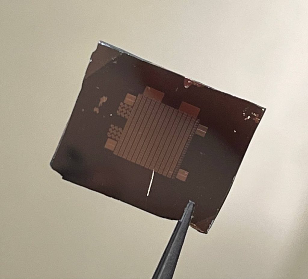
One of the initial samples I wirebonded successfully.
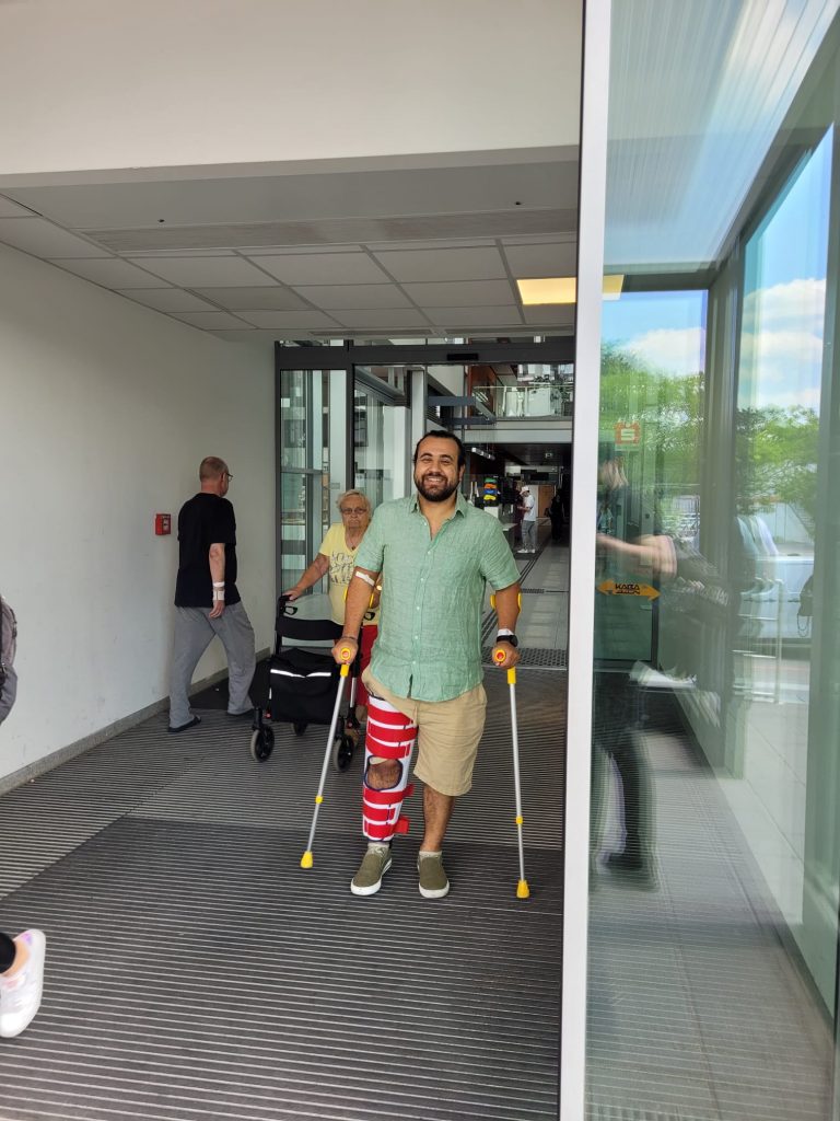
Recently, I was at ETH Zurich for my secondment. I was fortunate enough to be involved in an intriguing work in the emerging field of orbitronics and orbital torques. My daily work included struggling with the wire bonder to using a low temperature setup to measure spin-orbital torques at 25K to delving deep into the literature to find an explanation for my results. I was mentally tired at the end of the day.
Thankfully, there were a lot of opportunities for doing sports in and around the university. Marco (ESR3) was kind enough to lend me his bicycle. I biked to work multiple times a week and also explored the outskirts of Zurich on weekends. I was able to reconnect with my old passion of Taekwondo, thanks to the sports offer from ETH and ASVZ. The most interesting sporting event for me was the football cup organised by the Materials Department (D-MATL) of ETH Zurich. I participated as part of the Magnetars 2.0 team, consisting of fellow members from the lab and Prof. Gambardella himself who was by far the MVP for our team. There were a lot of memorable moments from the tournament including the skillful play of Matthias, the determination and grit of Marco, the masterful touches of Nicholas, the threatening runs down the wing by Min-gu and Enrique and the great tactical positioning by Annika and Laura. The moment of the day was however the long range goal scored brilliantly by Mark. Apart from these, the daily commute to the lab itself required me shed some drops of sweat since it is located on top of Honggerberg in Zurich. Overall, my stay in Zurich was filled with memorable moments in the sports field and also from scientific discussions in the coffee room, the lab, the canteen and any place imaginable. Keep watching this space for more details on my scientific work in Zurich.
Some pictures from my excursions on Marco’s bike and from the D-MATL football tournament.
I returned to Grenoble just in time to attend the PhD defense of Dr. Salvatore Teresi (ESR7 – the first SPEAR ESR to complete his PhD). I also participated in the Grenoble Ekiden (a relay marathon race) with my Spintec colleagues, thus continuing my involvement with sports. Even though I am physically destroyed quite often, my mental state is relaxed and mood is uplifted at the end of every sport session. In conclusion, do some sports if you can. It will be beneficial to maintain a healthy body but also a healthy mind.
The successful defense of Dr. Teresi (ESR7) and some pictures from the Grenoble Ekiden relay marathon.
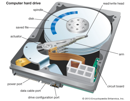
In the fascinating world of physics and electronics, the term “spin” of an electron holds a pivotal place. While it might sound like something out of a science fiction movie, the electron’s spin is a fundamental property that has revolutionized our understanding of the microscopic world and paved the way for groundbreaking technologies, particularly in the field of spintronics. This blog post aims to demystify the electron spin and introduce some spintronic devices like the Nobel Prize-winning discovery of Giant Magnetoresistance (GMR), which is responsible for the high storage capacities of modern hard drives. We will also explore some exciting applications and future prospects of spintronics.
While the term “spintronics” may have different connotations for different people, this blog post primarily focuses on providing a brief introduction to this field mainly from the perspective of data storage devices. However, the field expands into other domains, involving the science and technology of using the spin degree of freedom of charge carriers to store, encode, access, process, and transmit information. The field is extremely vast, and discussing everything is beyond the scope of this post.
Interest in spintronics was motivated by a longstanding belief that replacing charge with spin could yield significant advantages in terms of processing speed, energy efficiency, and device density on a chip. These advancements have become an absolute necessity in the 21st century considering the growing demand for energy in the information and communication sector. This demand is expected to consume 20% of global electricity by 2030.
Global energy forecast. Image adapted from ref. 1
The internet has grown exponentially over the last two decades. To put this into perspective, if the data stored on the internet today were printed on paper, it would form a stack reaching beyond the moon! This massive growth highlights the urgent need for more efficient data storage solutions, where spintronics could play a crucial role.
You can also checkout our project video which provides insights on the working principles of spintronics and how it is helping to tranform digital technologies.
What is electron spin?
To grasp the concept of electron spin, it’s essential to understand the basics of atomic structure. Electrons are subatomic particles that, along with protons and neutrons, make up an atom. These elementary particles all possess a quantum mechanical property called spin, which can be measured and has quantized values, including zero.
For the sake of understanding, students often visualize spin as the angular momentum associated with an elementary particle spinning or rotating about its own axis, like a spinning top or a planet. This mental picture is convenient but somewhat crude and incomplete.
Cartoon of spinning topCartoon of earth rotating
There are a few problems with this simplistic picture of an electron’s rotation about its own axis. This model cannot explain the quantization of spin angular momentum, as it suggests that spin should have continuous values rather than discrete ones.
Another problem arises when we try to calculate the spin angular momentum using this semi classical picture.
Where m0 is the mass of electron, vs is the speed of the surface of electron and re is the Lorentz radius of the electron given by,
Solving the above equation, we find that the speed of rotation on the surface of the electron exceeds 130 times the speed of light. Clearly, this would not be permitted by the Einstein’s theory of relativity.
What does this apparent fallacy imply? It indicates that the concept of spin is inherently quantum mechanical and cannot be described within the framework of classical mechanics. Furthermore, the electron cannot be visualized as a nearly point charge with the Lorentz radius.
Landau and Lifshitz, in their classic textbook on quantum mechanics wrote “[the spin] property of elementary particles is peculiar to quantum theory. [It] has no classical interpretation… It would be wholly meaningless to imagine the ‘intrinsic’ angular momentum of an elementary particle as being the result of its rotation about its own axis.”
Experimental and Theoretical Developments
Throughout the 20th century, numerous experiments and theoretical developments significantly enhanced our understanding of the electron’s spin. One of the most pivotal experiments was the Stern-Gerlach experiment in 1922, which demonstrated the quantized nature of angular momentum and provided direct evidence of spin. In this experiment, silver atoms were passed through a non-uniform magnetic field, resulting in the atoms being deflected in discrete directions rather than a continuous spread, indicating the presence of quantized spin states.
Stern-Gerlach experiment schematic and the image of the postcard sent by Gerlach to Bohr. Image adapted from ref. 3 and 4
Further theoretical advancements came with the development of quantum mechanics. Paul Dirac’s relativistic quantum theory in 1928 successfully incorporated spin into the framework of quantum mechanics, predicting the existence of antimatter and providing a more comprehensive understanding of the electron’s behaviour.
Experimental techniques continued to evolve, allowing more precise measurements of spin-related phenomena. For instance, the discovery of electron spin resonance (ESR) in 1944 enabled scientists to study the magnetic properties of electrons in various materials. This technique exploits the fact that electron spins can resonate in an external magnetic field, providing detailed information about the electronic structure of substances.
Another significant milestone was the development of the scanning tunneling microscope (STM) in the 1980s, which allowed for the visualization and manipulation of individual atoms and their spins on surfaces. This breakthrough opened new avenues for research in surface physics and nanotechnology.
These theoretical and experimental advances have collectively deepened our understanding of spin and its behaviour under different conditions. They have paved the way for modern applications in fields such as spintronics, where the manipulation of the electron’s spin is used to develop new technologies for data storage and processing. The interplay between theory and experiment continues to drive progress in understanding the fundamental properties of matter.
Spintronics: Electronics with electron spin
In the mid-20th century, it became clear that electron spin plays a fundamental role in magnetism. Every theoretical model developed to explain the physical origins of magnetism, such as the Bloch model, the Heisenberg model, and the Stoner model, invoked spin in some way.
While magnetism has always been closely linked with spin, in the late 20th century came a breakthrough realization: spin, either alone or in conjunction with charge, can be harnessed to process information. An electron can have one of two spin states: “spin-up” or “spin-down,” typically represented by arrows pointing up or down. This binary nature of spin makes it an excellent candidate for encoding information, similar to how binary code (0s and 1s) is used in traditional computing.
Image adapted from SPEAR Logo
This role had been traditionally delegated to the “charge” of an electron, not its “spin.” Over the last two decades or so, there has been burgeoning interest in augmenting the role of charge with spin, or even replacing charge with spin in information processing devices.
Comparison between conventional electronics and spintronics
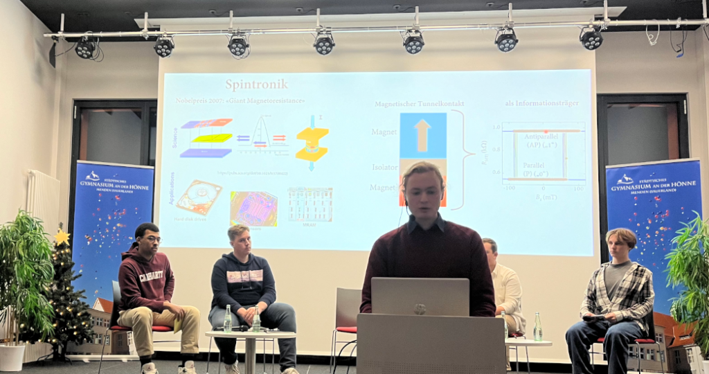
Giant Magnetoresistance
The discovery of GMR was a groundbreaking moment in the field of spintronics and in physics, achieved independently by Albert Fert in France and Peter Grünberg in Germany in 1988. Their work demonstrated how the resistance of multilayered magnetic structures could change dramatically in response to an external magnetic field. This discovery was so impactful that it earned them the Nobel Prize in Physics in 2007.
GMR is a quantum mechanical magnetoresistance effect observed in thin film structures composed of alternating ferromagnetic and non-magnetic layers. The resistance of these structures changes significantly in response to an external magnetic field.
Working principle of GMR
Layer Structure: The GMR effect is typically observed in multilayered structures where layers of ferromagnetic materials (like iron or cobalt) are separated by a non-magnetic spacer layer (such as chromium or copper).
Spin-Dependent Scattering: Electrons in ferromagnetic materials have spins that can be either parallel or antiparallel to the magnetization of the layers. The resistance of the material depends on the relative orientation of these spins.
Parallel Alignment: When the magnetizations of the two ferromagnetic layers are parallel, electrons encounter less scattering (i.e. current flowing through the layers will encounter lower resistance).
Antiparallel Alignment: When the magnetizations are antiparallel, the scattering increases (i.e. current flowing through the layers will encounter lower resistance).
Magnetic Field Influence: The magnetization of one of the ferromagnetic layers can be switched at will by applying a magnetic field. This change in resistance of the structure depending on the magnetization state of two ferromagnetic layers is the GMR effect, and it allows external control of the resistance state (high/low) of the structure.
Left schematic (adapted from ref. 5): GMR´s working principle, a spin pointing towards right (represented by black arrow at the bottom) will experience a higher resistance when travelling in a layer with magnetization pointing towards left (solid-pink arrow, pointing towards left) but the same spin will experience low resistance when travelling in a layer with magnetization pointing to the right (solid-pink arrow, pointing towards right). The vertical arrows pointing upwards represent the path of spin through different the layers. Right schematic (adapted ref. 6): GMR sensor reading individual bits
Applications of GMR
-Hard Disk Drives (HDDs): GMR read heads are used in modern HDDs. The ability to detect small changes in magnetic fields allows for the reading of densely packed data on the disk, significantly increasing storage capacity leading to HDDs with terabyte-level capacities
– Magnetic Field Sensors: GMR sensors are used in various applications to detect magnetic fields with high sensitivity. These sensors are used in automotive applications, industrial positioning, and consumer electronics.
– Biological and Chemical Sensors: GMR-based sensors are being developed for detecting biomolecules and chemical substances, taking advantage of their high sensitivity and specificity.
Giant Magnetoresistance and spin valves have not only advanced data storage technology but also opened new frontiers in sensor technology and spintronics. Their ability to manipulate and detect electron spin with high precision underscores their significance in both scientific research and practical applications. The continued development and application of GMR technology promise to drive further innovations in electronics and information technology.
Outlook
Looking forward, the field of spintronics holds immense promise for revolutionizing the next generation of electronic devices. Spin Transfer Torque Magnetic RAM (STT-MRAM) and Spin-Orbit Torque RAM (SOT-RAM) are emerging as potential replacements for traditional memory technologies, offering faster speeds, higher endurance, and lower power consumption. Beyond memory, spintronics is paving the way for innovative devices like the MESO (Magnetoelectric Spin-Orbit) device, which could lead to even more energy-efficient computing. These technologies are not just theoretical; they are actively being developed and hold the potential to transform everything from data storage to processing, enabling smarter, faster, and more sustainable electronic systems. The future of spintronics is bright, with the potential to push the boundaries of what’s possible in the digital age.
a) Schematic of STT b) Schematic of SOT based device c) Schematic of MESO device Adapted from ref. 7
References:
Jones, N. (2018). How to stop data centres from gobbling up the world’s electricity. Nature, 561(7722), 163–166. https://doi.org/10.1038/D41586-018-06610-Y
Bandyopadhyay, S. ., & Cahay, M. . (2020). Introduction to spintronics. CRC Press. https://www.routledge.com/Introduction-to-Spintronics/Bandyopadhyay-Cahay/p/book/9780367656447
Castelvecchi, D. (2022). The Stern–Gerlach experiment at 100. Nature Reviews Physics 2022 4:3, 4(3), 140–142. https://doi.org/10.1038/s42254-022-00436-4
How the Stern–Gerlach experiment made physicists believe in quantum mechanics – Physics World. (n.d.). https://physicsworld.com/a/how-the-stern-gerlach-experiment-made-physicists-believe-in-quantum-mechanics/
Application of GMR | Evgeny Tsymbal | Nebraska. (n.d.). Retrieved August 21, 2024, from https://unlcms.unl.edu/cas/physics/tsymbal/reference/giant_magnetoresistance/application_%20of_gmr.shtml
CALAVALLE, F., & CALAVALLE, F. (2022). Probing and tuning the electronic properties of low dimensional van der Waals materials. Ph.D thesis UNIVERSIDAD DEL PAÍS VASCO/EUSKAL HERRIKO UNIBERTSITATEA
Manipatruni, S., Nikonov, D. E., Lin, C. C., Gosavi, T. A., Liu, H., Prasad, B., Huang, Y. L., Bonturim, E., Ramesh, R., & Young, I. A. (2018). Scalable energy-efficient magnetoelectric spin–orbit logic. Nature 2018 565:7737, 565(7737), 35–42. https://doi.org/10.1038/s41586-018-0770-2
Recommended music to listen while reading: https://www.youtube.com/watch?v=OkHFGL1NOfA
Three years and one day ago, I flew from Madrid to Hamburg. I woke up at around 5 a.m. to take a plane that left me in the city of the moin and the Franzbrötchen around noon. When landing, the plane dived into the thick ocean of clouds that we had been hovering above for some time, and I found myself in a dark, rainy and dull city. I felt sad and alone. But before I could lose myself in that scary place, Olga came to pick me up from the airport. I still felt sad, but I was no longer that alone.
The next day, Kirsten met me just to show me the city centre, and again, under that continuous canopy of clouds, I felt slightly less alone, slightly more wanted. At that moment, I was scared of everything: my English, the place, my boss, the culture… Everything. And I am sure I was a very annoying kid who couldn’t stop complaining about the rain, the clouds and the wind, because it was easier to dislike everything than to stop and take a look at myself.
With time, more and more people came into my life, making, each of them, my life more worth living. First it was Vishesh, then Homero, Jonas, Roberto, André, Julia, Lukas, Jannis, Ali, Tim, Eva… And many others. With them I learnt how to live in another culture, how to be part of the world. I already knew how to live far away from my hometown, and also knew how to live in a big city! But I didn’t know I still had more to learn. Now I understand I will never stop doing it.
My PhD comes to an end. Not right now, as these Hamburg people cannot get rid of me so easily, but soon. I will most probably defend my thesis at the beginning of next year, but I will never leave behind the people I have met here and everything they have taught me.
I am now a less annoying kid than the one who landed on that 28th of August of 2021. I am a kid who has learnt to appreciate the rain, the clouds and the wind. I am a kid who knows that wir sind nichts aus Zucker.
So, this is not an attempt to say farewell to meine Perle, this is just the last stop before our final adventure together. This is just the beginning of the end.
Sometimes doing a PhD can get tough, challenging, sometimes you have to do your best to keep the motivation. But sometimes, you get to go to a conference in Brazil.
Attending the INTERMAG 2024 conference in Rio de Janeiro, at the third year of my PhD, has been an incredible experience and a pivotal moment in my academic journey. The opportunity to engage with leading experts in the field of magnetics, exchange ideas, and broaden my network was invaluable. Presenting my work through an oral presentation and two posters allowed me to receive a wealth of feedback and new perspectives. The mix of in-depth technical sessions and the chance to connect with peers from around the world provided a fresh perspective on my work and opened doors to new collaborations.
Beyond the academic benefits, the vibrant atmosphere of Rio added a unique energy to the conference. The mix of professional development and the chance to enjoy the city’s unique beauty made this experience a memorable and impactful part of my PhD journey.
In addition to conducting research, presenting research is a crucial part of a PhD student’s life. Whether in the form of posters or talks at conferences, presenting your research is as important as the results themselves. An engaging presentation increases the likelihood that your work will be appreciated and, more importantly, understood. The most important goal is to improve the accessibility of knowledge. In particular, intuitive graphics and diagrams can be used to convey content more effectively. That is why we invest a lot of time and effort in creating high-density graphics. Depending on the type of content, such as posters, presentations or papers, different standards are applied.
In the case of a poster, the aim is to attract the interest of passers-by. The content must be visually appealing to attract people casually passing by. Given the limited space, the content must be well condensed without visually overwhelming the viewer. This is where an unconventional design can score points and allow for more creative freedom.
The original plots on the left were transformed and merged using a vector graphics programme into the figure on the right, which was used in a poster I presented at ICM24 in Bologna.
When designing a presentation, you are not limited by space, but by time, which requires well thought-out storytelling. In the case of a presentation, the focus is on clarity to effectively convey knowledge to the audience, while at the same time being visually appealing to keep their attention. It is important that the slides support the presentation and are not the presentation itself.
This type of image is intended to provide a concise and easy-to-understand overview and timeline of the processes used to support the text version.
Figures for papers are very different, where information density needs to be maximised. Since the number of pages and figures is usually very limited, careful planning is required to decide what content needs to be presented. As figures are often made up of different sub-plots, the structure must be rigorous to ensure that the content is intuitively understandable and the relationships are clear. I want wo use an example from my Master thesis, where represented the process steps to fabricate the samples:
This type of image is intended to provide a concise and easy-to-understand overview and timeline of the processes used to support the text version.
Creating figures and schematics allows me to use my creative and graphic design skills, which is a nice balance to my working day. The process of translating complex data into clear and engaging visuals is both challenging and fulfilling. Creating these graphics allows me to combine scientific accuracy with an artistic touch, making the information more accessible. Whether I’m designing a poster, presentation or figure for a paper, I find satisfaction in the careful attention to detail required. This combination of creativity and science makes presenting research an enjoyable and meaningful part of my job.
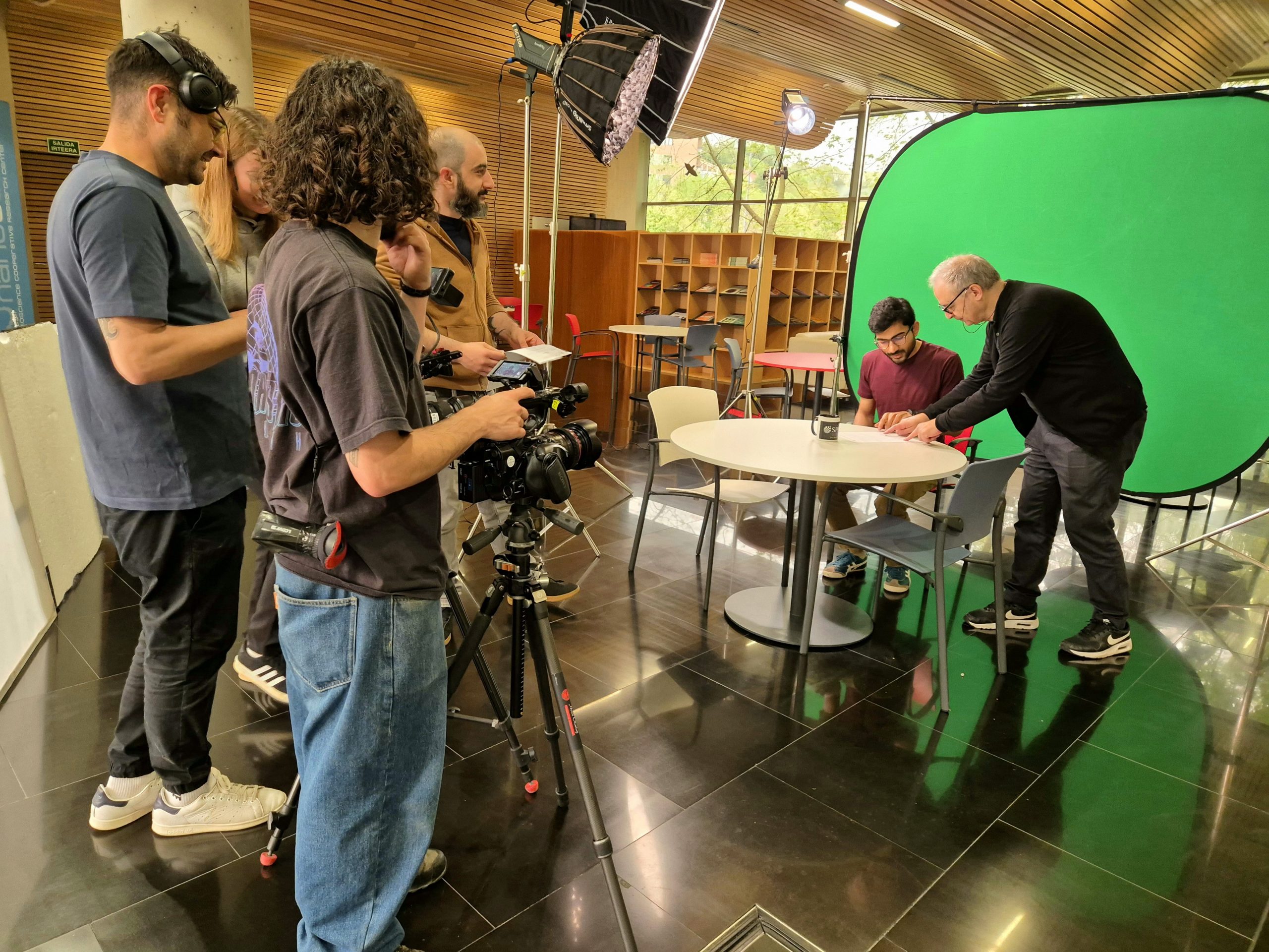
Behind the Scenes: The making of our SPEAR outreach video
Working on our SPEAR outreach video has been a thrilling and intricate adventure. I volunteered to coordinate this project, but there’s no way it would have been possible without the awesome support and guidance of our project manager, Eli. Big shout out to Eli and all our lovely ESRs!
I jumped in because I love making videos. This outreach video was the perfect way to satisfy my passion while making a meaningful contribution to our project – what better deal than this?
From scripting to finding the right video agency, and even acting in the video, I had the chance to oversee everything. Though we’re still in the post-production phase, I wanted to share a sneak peek behind the scenes, highlighting the creativity, collaboration, and coordination that went into making this video.
Scripting and Conceptualization
The first task was to develop the concept and script for the video. Our project focuses on spintronics, with ESRs working on various subtopics, some closely related and others a bit more distant. For the video, we wanted to move away from the usual “this is our project, and here’s our cool lab” format. Instead, we aimed to create something more meaningful and engaging for young viewers, sparking their interest in the field of spintronics.
The idea was to give the video a documentary-style approach, starting with the basics of electronics and its ubiquitous presence in both personal and commercial sectors. We wanted to illustrate how technology is woven into every aspect of our lives, which naturally leads to a discussion on the resulting excessive energy demands. This would smoothly transition into the need for better, faster, and more energy-efficient technology solutions—enter spintronics.
In the video, we briefly explain that spintronics leverages the spin of electrons to achieve these advancements. From there, we feature short segments where ESRs working on different subtopics within spintronics briefly describe their specific projects while connecting it to real-world applications and challenges.
Our goal was to create a narrative that not only informs but also captivates, making the viewer understand and appreciate the importance and potential of spintronics in addressing modern technological and energy challenges.
Finding the Right Video Agency
Finding the right video agency was a journey in itself. We reached out to contacts all around, from Zurich to the UK, with the initial idea of possibly shooting the video at various locations, showcasing the different labs involved in our project. However, we quickly ran into a series of challenges, from budget constraints to scheduling conflicts with the video agencies.
Additionally, coordinating the schedules of all the ESRs, each heading off to their respective secondments, made availability a major hurdle. After extensive searching and coordination, we finally found an agency in San Sebastian. Fortunately, they had some dates available just before I was set to leave for my secondment in Zurich. It felt like everything finally fell into place, allowing us to move forward with our video production plans.
Working with the Video Agency
Once we found the right video agency, the real fun began. I really liked the director from the start, and once the script was ready and he was happy with it, we dove into the details of how the video should be shot. Since we decided to film at the nanoGUNE, where I’ve been working for the past two years, I had some interesting ideas about the different scenes and locations. We shared these ideas with the director, and despite a small communication gap (my Spanish isn’t the best), he immediately understood our vision. It felt like he could read my mind! Not only did he enhance the ideas, but he also introduced some fantastic new ones.
Filming Day
Filming day was both exhilarating and exhausting, starting bright and early at 8 am and wrapping up around 7 pm. I was filled with excitement and a bit of nervousness. At times, I even forgot the smallest lines! The first scene was nerve-wracking, but as the day went on, I became more comfortable with the crew and the filming process.
Eli was always around, ensuring that every line was delivered correctly and without grammatical errors. Her presence and support were invaluable throughout the day. The whole crew was fun to work with, and the director was especially supportive.
There were some memorable moments that really stood out. In one scene, I was supposed to walk down a busy street, with the chaos of pedestrians in the background. For each take, we had to wait for the traffic light to turn green for pedestrians so that the timing and background would be just right. The shot also involved some tricky handheld camera movements and changes in focus. We faced a series of amusing challenges – sometimes I walked too fast, other times the camera lost focus, or there simply weren’t enough pedestrians crossing the street. Each of these little hiccups made the day more memorable and added a lot of laughter to the mix.
Despite the long hours, I enjoyed every moment of the shoot. The director’s guidance and the team’s camaraderie turned what could have been a stressful day into an incredibly fun and productive experience. By the end of the day, it felt like we had created something beautiful, capturing not just the essence of our project but also the enthusiasm and dedication behind it.
We’re now in the post-production phase, and the excitement continues to build. The final touches are coming together, and I can’t wait to see the finished video and share it with everyone. Stay tuned for its release!
The best summary of the last eight months would be my love-hate relationship with my luggage. Since every few weeks, I had to go somewhere new, I always had to have it at hand. This was a daily reminder that I was leaving in a few days, meaning hours by train or on a plane, managing tickets, eating on the road, and the worst, more goodbyes. But it was also a reminder that a new chapter was coming: new people, new places, and new adventures. Between three secondments, conferences, vacations with friends, and short visits to Halle, I felt I was always arriving or about to leave. Therefore, I feel blessed by science to have managed to meet the most amazing groups of people.
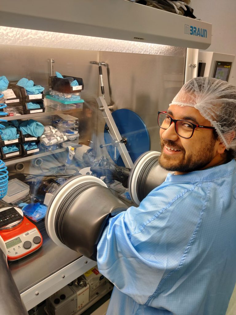
A very unexpected part of the secondment was the eye-opening time at SIMUNE. This industrial secondment completely changed my perception of what it means to work for a company. The team welcomed me in a very natural process and gave me the tools and time to learn the basics of their project. We were able to finish the secondment with a working feature on their code, which, aside from the feeling of success, showed me the complete process of implementing new features into an existing code. From reading to writing documentation and reviewing good coding practices, my coding is now at a whole new level. I discovered the fun and excitement of going from the planning to the final product with a user-oriented goal, which comes with challenges that an academic paper will never see. The biggest surprise was the day-to-day working process, which included a lot of teamwork to solve minor problems quickly, daily update meetings, and weekly demo presentations. This showed me a whole new strategy to work on a project. On top of that, the connections we built through teamwork, problem-solving, and commenting on small stuff during the short but lovely coffee breaks are something that helped me work confidently.
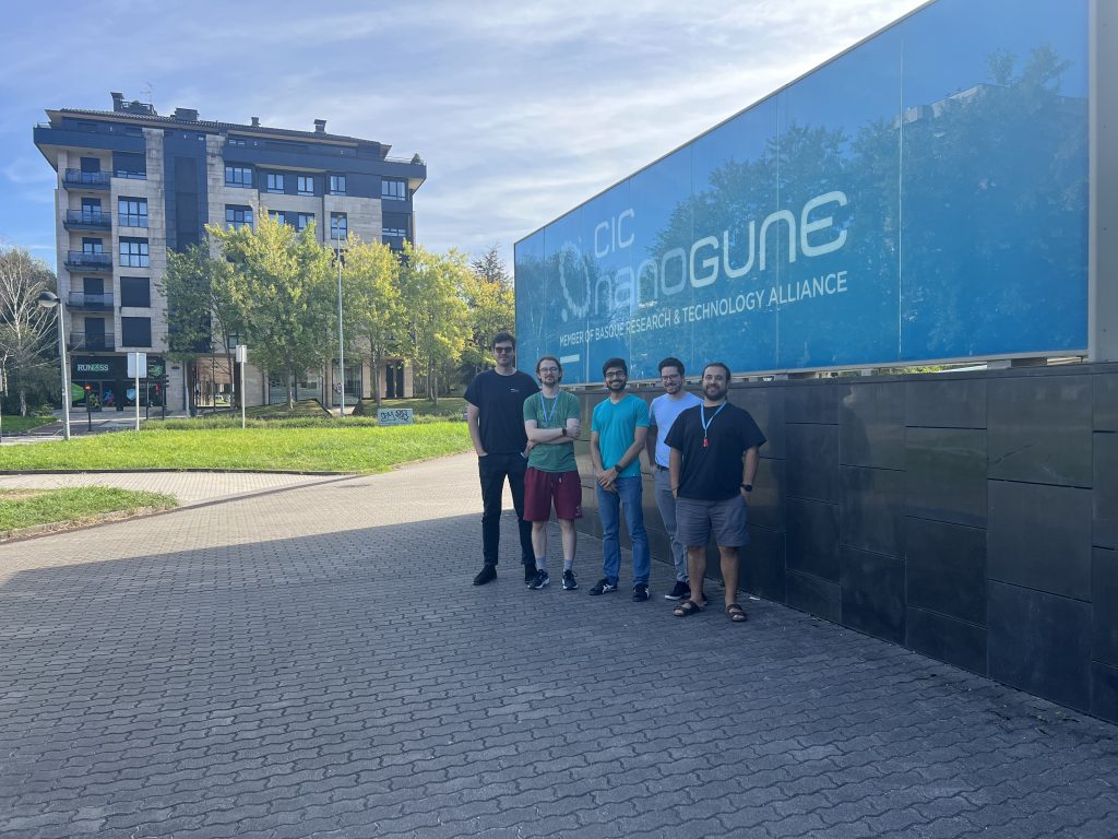
Nanogune group
Of course, all of these fun and productive times were alongside the recovery from the knee surgery a few months before going to Spain. This process was particularly eased by the beautiful beach in Donosti, the location of my first two secondments. Swimming in “La Concha” and “Ondarreta” was the best I could have done to train my leg muscles. Now I am fully recovered, even though I still need a few more sessions of physiotherapy, I can finally enjoy long bike rides and, who knows, maybe a run every now and then.
Spintec group
Not everything during the secondments was about working in SIMUNE, nor drinking and eating delicious local products in Donosti and Grenoble. I was also trained in various sample production techniques and benefited from incredible discussions, where I now understand my calculations from a whole new perspective from an experimental point of view. We also got two very interesting ideas for collaborating with the theoretical group at Spintec.
As always, I cannot be happier with how the project is going and cannot wait to see how my life is going for my next blog post. Prost, Salud, and Santé to Halle, Donosti, Grenoble, and the SPEAR program!!
In March, I had the opportunity to travel to Minneapolis, USA, to attend the APS March Meeting 2024. The APS March Meeting is renowned for bringing together experts in condensed matter physics and quantum physics from around the world. It was also my first time participating in such a prestigious international conference during my PhD studies.
At the conference, I presented a talk titled “Nuclear Magnetic Resonance with a Single NV Scanning Probe.” The focus of my presentation was on showcasing the innovative potential of using a scanning NV (nitrogen-vacancy) probe to perform nanoscale NMR (Nuclear Magnetic Resonance) measurements. This technology represents a significant advancement, as it enables high-resolution imaging at the nanoscale, which can be applied across a wide variety of scientific domains.
Figure 1. ESR 13 Zhewen XU at 2024 APS March Meeting
After the conference, my colleague Chaoxin and I embarked on a memorable trip along the East Coast of the United States. Our journey began in Boston, where we explored the historic Freedom Trail. Figure 2 captures the start of our adventure on this iconic trail, which is rich with American history and landmarks.
Figure 2. The start of the Freedom Trail in Boston
Figure 3. Ismael and I on the top of Rockefeller Center
From Boston, we headed to Washington DC and then to the New York City. One of the highlights of our visit was going to the top of Rockefeller Tower. The view from the observation deck was breathtaking, offering a perfect view of the sprawling city below. During our time at Rockefeller Center, I have met Ismael (ESR 10). Afterwards, we had our pleasant dinner at a shrimp restaurant (from the movie “Forrest Gump”) near the Times Square.
July 5th will be exactly two years since I started my PhD, and I feel like everything passed by in the blink of an eye, and I have a lot to do in such a short remaining time. It’s been tougher than I expected, but I believe that the key is to stay focused and motivated. After all, a friend once told me that the PhD is not a plug-and-play journey, and it’s unreasonable to expect things to work smoothly!
Aside from these struggles, I’ve attended a workshop on 2D materials here in Gothenburg, organized by SIO Graphene. Although the topic is not related to my area of expertise, it was super useful to listen to people from industries in Sweden talk about their work, and the fact that it was a small workshop made it easy for me to talk and mingle with people and make connections with them, compared to a big conference. If I’ve bored you with my words, here is a fun game: Find me in the picture below!
SIO Graphene meeting in Gothenburg!
I’m getting ready for my secondment at IMEC, Leuven. I will start on July 1st and will be there until the end of September. Without question, it will be a great experience for me, and I’m looking forward to seeing Kaiquan and Xinyu there!
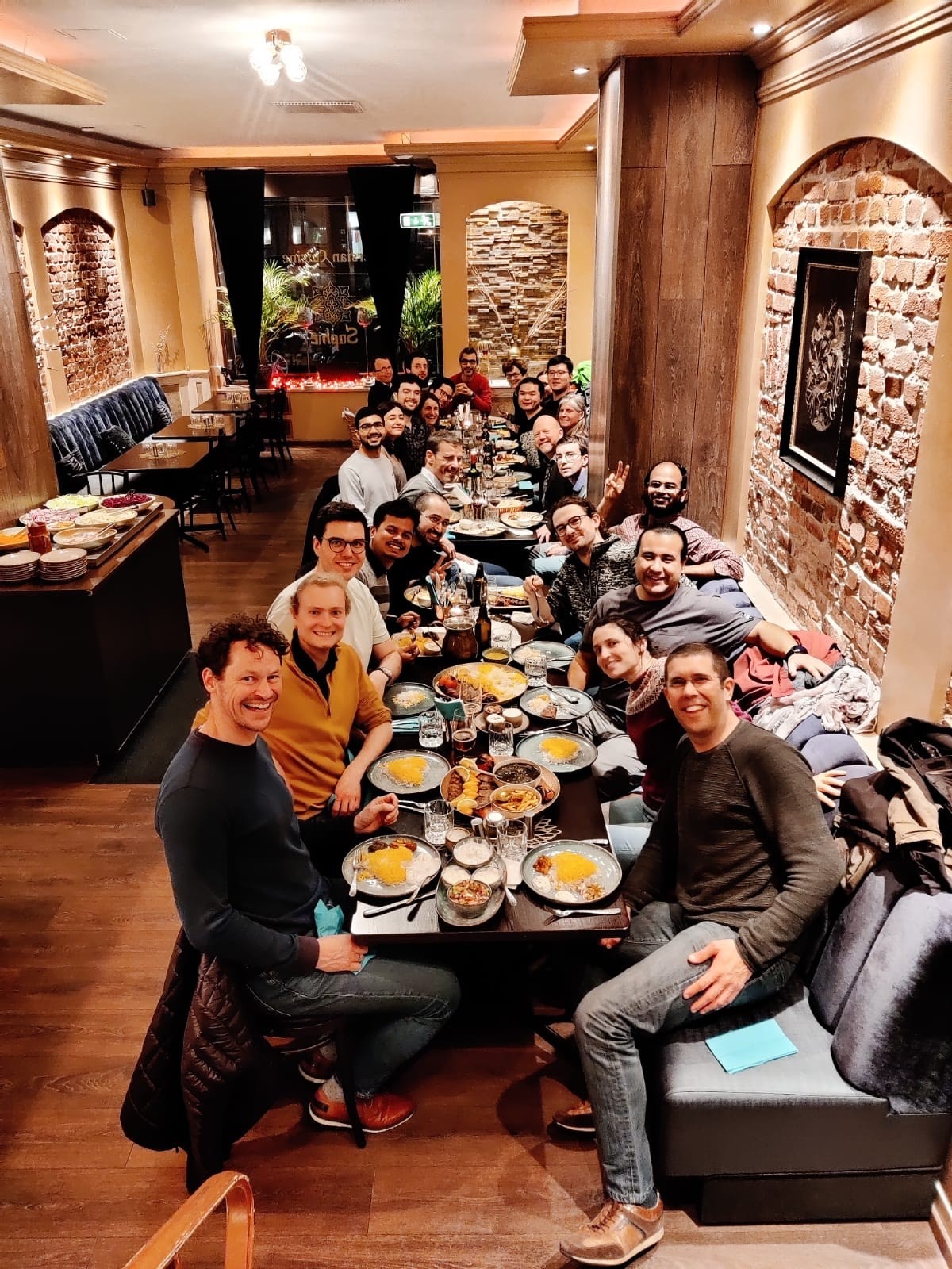
Hello readers. My last few months have included a lot of developments in my life. The nice moments were when we had the SPEAR meeting this time in Hamburg, Germany. It was fun to host my fellow ESRs and show them around. As you can see, we had a lot of fun exploring the Hamburg city, going for dinners and even playing laser tag!
Regarding science, I have had nice results and we are currently finishing the manuscript. I also had nice discussions with Ismael about possible implementations with respect to reservoir computing of my system and in the process learnt a lot about the topic. It was fun to host Ismael again for his last bit of secondment period at Hamburg where he tried to get atomic resolution using the STM!
I am looking forward to attending the ICM conference in bologna in July and also visiting cool places like the Dolomites and Tuscany!
During my time in Zurich, I was heavily involved in studying samples provided by a research group at Spintec. Our focus was to detect skyrmions in these samples. It was like solving a puzzle every day, trying to unlock the secrets hidden within. We used NV magnetometry as our main tool, which allowed us to measure magnetic fields at the nanoscale with incredible precision. Zhewen, the ESR of our consortium at the startup, played a crucial role in helping me navigate the intricacies of the NV tool, providing invaluable insight and support along the way.
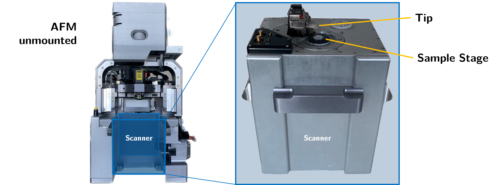
Outside of work, I made sure to explore Zurich’s academic offerings. One outstanding experience was a visit to ETH Zurich, an excellent university. I visited Pietro Gambardella’s lab where I had a good time with Marco and Niklas, the two ESRs of our consortium in that lab, and I learnt a lot about atomic force microscopy (AFM), which was quite exciting.
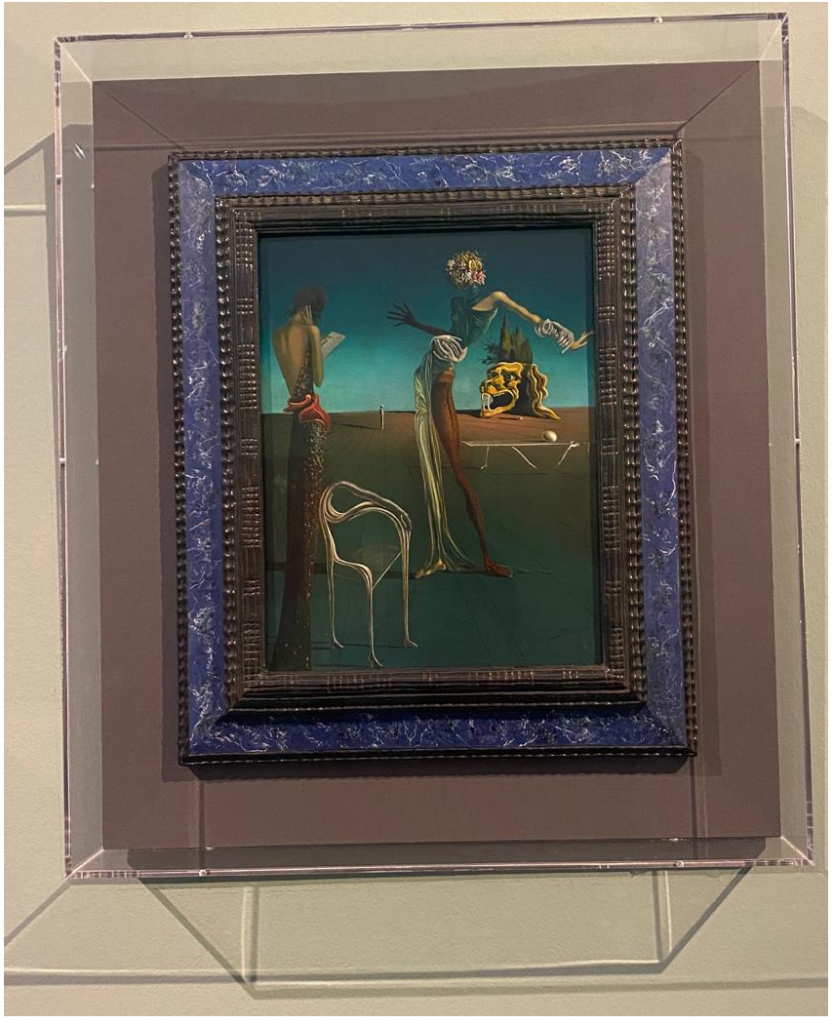
During one of the weekends, I decided to visit the Kunsthaus, eager to immerse myself in the world of art. Walking through the halls, I came across some important paintings from the Impressionist movement or the more recent Salvador Dalí. It was a surreal experience to see these famous pieces up close, but what really caught my attention was the work of De Chirico, an artist I have always admired. His surrealistic landscapes and enigmatic compositions have always fascinated me, and seeing them in person was a highlight of my time in Zurich.
When I was not in the lab or exploring the art scene, I took the opportunity to immerse myself in Zurich’s cultural offerings. Lazy walks along the Limmat River allowed me to take in the city’s unique blend of old and new, while exploring local markets and trying different cuisines added layers to my experience.
However, what really made Zurich special for me were the people, everyone I met was friendly and welcoming. These personal connections made my time there truly memorable.
As my time in Zurich ended, I couldn’t help but feel grateful for the experiences I’d had. From the scientific discoveries to the cultural immersion, it was a journey I won’t soon forget.
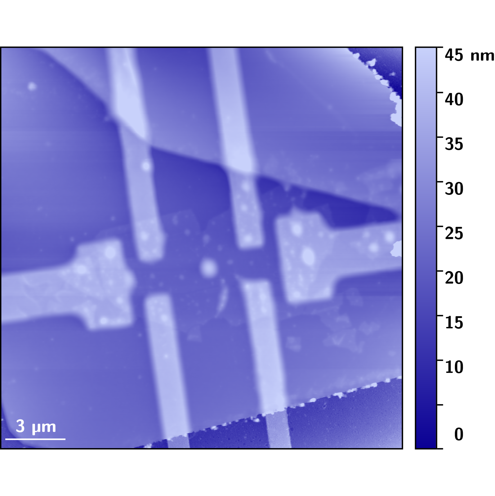
Here are two pictures that represent two memories of my experience, the first skyrmion I found and a painting of Salvador Dalí.
Quantum sensing magnetometer and its spatial resolution
In recent years, the field of quantum sensing[1] has witnessed a revolutionary advancement with the emergence of nitrogen vacancy (NV)[2] centers as versatile and highly sensitive quantum probes. NV centers, found in diamond crystals, exhibit unique quantum properties that make them ideal candidates for a wide range of sensing applications.
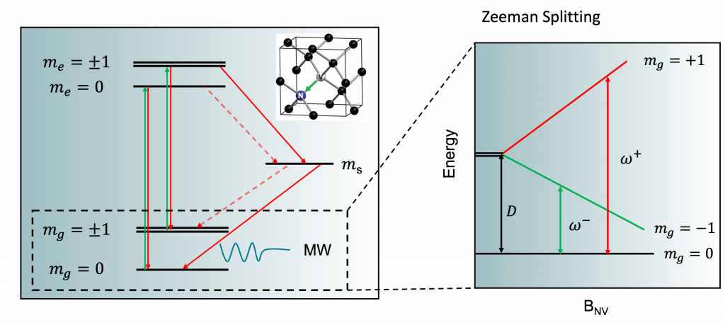
The NV center consists of a nitrogen atom adjacent to a vacancy in the diamond lattice, along with two neighboring carbon atoms. It can be interrogated using optical techniques. When illuminated with green light, NV centers absorb photons and enter an excited state. Subsequently, they relax back to their ground state, emitting red fluorescence (c.f., Figure 1, box 1). The intensity and polarization of this fluorescence depend on the spin state of the NV center, which can be manipulated and read out using microwave and optical techniques. By precisely measuring changes in fluorescence, NV centers can be employed to sense and characterize various physical phenomena. On the other hand, as a single Q-bit, the electronic ground state of the NV center consists of a triplet spin configuration, i.e., m_s = 0, ±1. When no external magnetic field is applied, |-1> and |+1> energy levels are degenerated. However, when an external magnetic field is introduced, the energy levels experience a Zeeman splitting due to the interaction between the electron’s magnetic moment and the magnetic field. According to the Zeeman effect, the energy levels shift in energy, with the amount of splitting depending on the strength and direction of the magnetic field (c.f. Figure 1, box 2). By precisely measuring the energy splitting and phase differences between spin states, NV centers can be employed as ultra-sensitive sensors in diverse fields such as magnetometry, bio-imaging, quantum information processing.
Figure 1. NV center energy diagram and Zeeman splitting
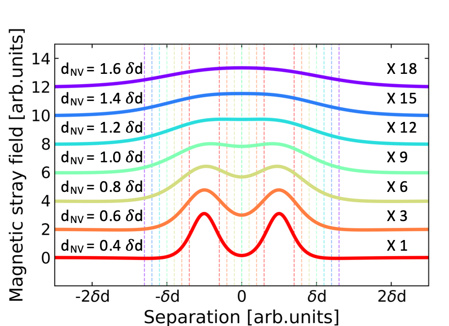
Although NV center offers unparalleled sensitivity in real space imaging, one of its limitations is the requirement for close proximity to the sample surface. This constraint poses challenges for imaging finer structures that require a lower stand-off distance. The spatial resolution of Scanning NV magnetometry (SNVM) depends on the sensor-to-sample distance dNV , as opposed to optical microscopy, whose resolvability is constrained by the diffraction limit, and other quantum sensing technique such as scanning superconducting quantum interference devices microscopy (or scanning SQUID microscopy) , whose resolvability is limited by the sensor size. Figure 2 shows the change of the z-component of magnetic stray field originating from two dipoles[3] separated by distance δd measured by NV at different dNV .
Figure 2. The SNVM measured z-component magnetic stray field above two dipoles separated by distance δd is modified by the sensor to sample distance dNV. At dNV = δd (light green curve), the FWHM of individual dipole equals to the separation between two maxims. Rainbow color sequence represents the different dNV , from 0.4 δd to 1.6 δd at each 0.2 δd interval. Stray field curves have been vertically offset for clarity and have been multiplied by a given factor to compensate for the weaker signal due to the large dNV .
It is evident that the peaks from two separated magnetic dipoles can be well resolved at small sensor-sample separation (dNV in the range of 0.4 to 0.8 of the dipoles separation δd). When dNV approximates δd, the distance between the two peaks equals the full width at half maximum (FWHM) of the stray field distribution curves. It makes distinguishing between two individual dipoles difficult. Beyond this point, the two magnetic dipoles can not be resolvable any longer. Analogous to the Rayleigh criterion, the spatial resolution in SNVM is defined as the smallest distance between NV and sources to be resolved.
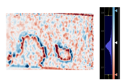
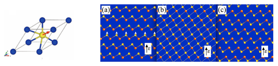
Figure 3. Images of a room temperature multiferroics bismuth ferrite (BiFeO3) by scanning NV magnetometry at different NV-to-sample distance. With decreasing standoff distance dNV, the spin cycloid (‘zig-zag’ shape patterns) can be well resolved.
Figure 3 illustrates the improved spatial resolution of SNVM through imaging the widely studied room temperature multiferroic material bismuth ferrite (BiFeO3)[4-6], known for its non-collinear antiferromagnetic spin cycloid that has garnered significant research interest in recent years. By shifting the NV center 21 nm closer to the surface of the BiFeO3 sample, the intricate ‘zig-zag’ pattern of the spin cycloid becomes clearly discernible.
In conclusion, the improved spatial resolution of scanning NV magnetometry represents a significant technological advancement with far-reaching implications across scientific disciplines. Through innovative techniques and methodologies, we have pushed the boundaries of spatial resolution, enabling nanoscale imaging of magnetic fields with unparalleled precision. As this field continues to evolve, scanning NV magnetometry promises to revolutionize our understanding of magnetism, quantum phenomena, and biological systems, paving the way for transformative discoveries and technological innovations.
[1] Degen, Christian L., Friedemann Reinhard, and Paola Cappellaro. “Quantum sensing.” Reviews of modern physics89.3 (2017): 035002.
[2] Degen, Christian L. “Scanning magnetic field microscope with a diamond single-spin sensor.” Applied Physics Letters 92.24 (2008).
[3] Lima, Eduardo A., and Benjamin P. Weiss. “Obtaining vector magnetic field maps from single‐component measurements of geological samples.” Journal of Geophysical Research: Solid Earth 114.B6 (2009).
[4] Gross, Isabell, et al. “Real-space imaging of non-collinear antiferromagnetic order with a single-spin magnetometer.” Nature 549.7671 (2017): 252-256.
[5] Haykal, A., et al. “Antiferromagnetic textures in BiFeO3 controlled by strain and electric field.” Nature communications11.1 (2020): 1704.
[6] Chauleau, J-Y., et al. “Electric and antiferromagnetic chiral textures at multiferroic domain walls.” Nature materials 19.4 (2020): 386-390.
On the similarities of chip design and the icing of cakes
I recently had the opportunity to present my research project in the form of a cake thanks to the PhD workshop at Nanogune. The humble poster is a tried-and-true method for relaying research output, but the cake is an underappreciated medium for the same. A great deal of information can be conveyed with the skillful application of icing, and the careful implantation of chocolate chip impurities in the amorphous sponge matrix. Pictured here (centre cake) is my research project, in icing. The graphene, a honeycomb of black icing balls, the gold contacts, a honey-coloured sheet of icing, and the silicon wafer a honey flavoured layer of nanometre thin sugar. Cooking and explaining my project like this was a surprisingly fun idea, and a creative way to convey information and have a tasty snack.
It makes one think that fabricating chips, something I also do on occasion, is much like baking a cake. In both cases you follow a certain recipe, carefully mix the ingredients, and bake at 1200C for 8-12 hours. In the end you emerge with something round and tasty, and that’s when the fun really begins! An icing of sugar or elemental gold, to really make your work shine. All that’s left is to carefully cut it up and share among friends and collaborators.
Recently, I have made Spintec my new home. Or workplace. It’s hard to differentiate sometimes due to the kind and helpful colleagues who are always ready to discuss life over a cup of coffee. Spintec is an interesting place since it brings together researchers from different fields of magnetism and spintronics community at different stages of their career. So, it doesn’t come as a surprise to me that Spintec hosted the kick-off for the huge PEPR SPIN project this January. Funded by the Agence Nationale de la Recherche (ANR), PEPR SPIN (Link to their website) aims to support research and innovation in the field of spintronics to achieve energy efficient, fast, and sustainable technology.
Many prominent researchers from all around France gathered in one place to celebrate the launch but also to share ideas and foster collaboration. The highlight of the day were two very interesting talks. The first one from the 2007 Nobel Laureate for the discovery of the giant magnetoresistance (GMR), Albert Fert about how the field of spintronics has developed over the years and the intriguing future potentials of upcoming phenomena and technologies. The second talk was from the co-founder of Spintec and a well-known name in the world of spintronics especially magnetic random-access memories (MRAMs), Bernard Dieny. He talked about the plethora of applications where magnetism and spintronics could be applied ranging from microelectronics to healthcare. If you are interested in how memory works in a computer and how does spintronics fit into memory technology, check out this post (Link to post).
The talks helped put my own research in perspective to the broader picture. As a student, the next most important thing for me was the food. It helped recover the calories that I spent understanding the talks given in French.
2007 Nobel Laureate Albert Fert talking about Spins!Talk of Spintec co-founder Bernard Dieny about application of spintronics in current technology
In the evening, we were welcomed at the Musée de Grenoble for the gala evening. I got the opportunity to interact with colleagues from different research centers in Grenoble and from different cities of France. I like these events since they allow us to discuss and get acquainted with each other in an informal setting. Sharing their love for science, food and art, hundreds of researchers enjoyed an evening away from experiments, data, and research papers. Although I am sure, there were a lot of scientific discussions that were casually brought in.
Memory Hierarchy – How does computer memory work ?
It’s 5pm on a Friday evening. I am done for the week. I save my half-completed article and prepare to leave. A fleeting thought says – “How is my file saved? How is data stored and accessed in a computer?” In this post, I try to answer these questions and understand how memory works in our computers with some examples. The file I saved is broken down into numerous bits or binary digits (0 or 1) and stored in memory units with each memory unit having either 0 or 1. Most computers are structured as a pyramid with the central processing unit (CPU) at the top as shown in figure 1. As we move downwards, we encounter short-term memory for frequently accessed tasks followed by long-term memory for permanent storage. While short-term memory is fast (5000-6000 megabytes per second) and has a smaller capacity (a few gigabytes) [1,2], long-term memory can be huge (a few terabytes) but is extremely slow (around 550 megabytes per second or less) [3]. Let’s take a look at the long-term or storage memories first.
Figure 1:The memory hierarchy or memory pyramid
Two broad technologies exist for long-term storage – hard disk drive (HDD) and solid-state drive (SSD). HDD stores data in magnetic domains in layers of magnetic film deposited on a rotating disk as shown in figure 2. Writing and reading is achieved by a read/write head that can read the magnetic state of the domains. This technology was introduced by IBM in 1950s. HDDs are non-volatile and can retain data even after being powered off [3].
Figure 2:Internal structure and components of a hard disk drive. Information is stored in the magnetic state of the magnetic domains and is read or written by the read/write head.
Figure 3:A floating gate transistor which is the basic building block of NAND Flash. A potential applied on the control gate results in transfer of charges from the transistor channel to the floating gate or vice-versa.
SSDs are based on a technology known as NAND Flash [4,5] developed by Fujio Masuoka at Toshiba in 1980s [6]. The basic building block of NAND flash is shown in figure 3. A potential difference between source and drain creates a channel of electron flow between them. Depending on the voltage applied at the control gate on top, some electrons are removed from or trapped in the floating gate. The presence or absence of the electrons results in a change in the resistance state of the device. Millions of such devices are arranged in a crossbar array to manufacture modern SSDs [3,7,8]. SSDs are 10 times faster than HDDs since they do not any mechanically moving parts. Although more expensive than HDDs, SSDs are used where high data transfer speeds and lower delays are desired. In case you haven’t already figured it out, modern thumb drives or flash drives are also based on the NAND flash technology. Most modern laptops and computers use SSDs for permanent storage whereas big data storage farms use a combination of HDDs and SSDs.
Figure 4:Cross-section of a DRAM chip and its cell array. Periphery logic is used to control the read, write and flow of information to/from the chip. Cross-section of the cell array shows the transistor and the capacitor of the 1T1C structure.
HDDs and SSDs are located at the bottom of the memory pyramid since they have huge memory capacity but slow access speeds. As we move up the pyramid, we come across dynamic random-access memory (DRAM) which is also popularly known as RAM. Also known as the main memory of the computer, DRAM stores the data of currently running programs. As the name random-access suggests, the data at any location in a DRAM can be accessed at any time. It was invented by Robert Dennard at IBM in the 1960s. The basic memory unit in a DRAM consists of a transistor and a capacitor in a 1T1C structure (shown in figure 4). Fully charged and completely empty capacitors denote 1 and 0 respectively. The source of the transistor is connected to the bitline (BL), the drain to the capacitor and the gate is connected to the wordline (WL). If we want to write a 1, the WL is opened, and the transistor is switched on. Electrical charges can now flow from the BL to the capacitor until it is fully charged. The transistor is then turned off and the charge in the capacitor is isolated. However, the charges are not perfectly isolated and leak out over time. The capacitive memory then must be re-written after a certain period [9]. Thousands of these 1T1C structures are arranged in arrays called banks. Multiple banks are combined to form a chip. Multiple parallelly working chips are combined to form the DRAM. DRAM has a capacity of a few gigabytes and access times in 10s of nanoseconds.
Figure 5:An SRAM chip
As we move further up in our memory pyramid, we come across cache memory. Cache memory stores frequently used instructions and data to improve computation time. Cache memory is implemented by a technology called static random-access memory (SRAM) (shown in figure 5). The memory unit of the SRAM is implemented by a combination of six transistors (6T). Since the operation of SRAM does not include the charging and discharging of a capacitor, it is faster than the DRAM. However, 6 transistors in a single memory unit in SRAM increase its cost and reduce the number of memory units that can be squeezed in a given area [10–12]. Cache memory is often referred to as “on-chip memory”.
What happens when I run a game, a software or just open a file?
Imagine I want to play the latest Assassin’s Creed on my computer. The game itself is installed in permanent storage (in the SSDs). When I run the game, the CPU sends around a lot of instructions to control the flow of data. The information is copied from the storage to main memory (to the DRAM). Remember the big “LOADING……” bar at the start? This transfer is necessary to reduce the latency while running the program and the reason behind minimum RAM requirements for all games and software. Depending on what part of the game you are currently playing, a part of the data is copied to the cache memory. Then, a part of that data on the cache is copied to the CPU registers and processed by the CPU. Now, imagine if the memory pyramid doesn’t exist and the CPU is forced to run the program directly from the permanent storage. Since the permanent storage is extremely slow compared to the cache memory, your agile assassin would be moving slower than a tortoise. Here are some videos (Video 1, Video 2) on YouTube that can help you understand more about how memory works in a computer.
How does spintronics come into the picture?
Multiple transfers of data make up most of the energy consumption of a computer. DRAM and SRAM are volatile memories which means once you turn off the power, all their data is lost and their memory needs to be re-written once they are turned on again. Also, as the size of transistors continues to decrease, the energy loss in terms of leakage current increases significantly. Current research is focused on replacing DRAM and SRAM with non-volatile technologies which can store data without the need for continuous power supply and have minimal leakage. One of the most promising solutions is to store data in magnets or magnetic devices. This has led to the development of magnetic random-access memories (MRAM). Spin transfer torque MRAM (STT-MRAM) products from Everspin technologies is already available in the market [13] and can compete with DRAM for certain applications. Meanwhile, spin-orbit torque MRAM (SOT-MRAM) [14,15] continues to garner interest from academia and industry and can potentially compete with SRAM in certain applications. Novel concepts for domain wall [16] and skyrmion-based [17] devices that can find their applications as CPU registers are also under development. While we continue to find solutions to improve our current computing scheme, there are plenty of emerging computing schemes that can overhaul the whole computing landscape. Check those out in previous posts (Maha’s blog, Marco’s blog, Paolo’s blog).
If you found this useful and/or would like to discuss further, don’t hesitate to contact me on LinkedIn.
References
[1] DDR5 | DRAM, https://semiconductor.samsung.com/dram/ddr/ddr5. [2] DDR5 SDRAM Datasheet and Parts Catalog, https://www.micron.com/products/dram/ddr5-sdram/part-catalog. [3] DC600M Enterprise SATA 3.0 SSD – 480GB – 7680GB – Kingston Technology, https://www.kingston.com/en/ssd/dc600m-data-center-solid-state-drive. [4] C. Monzio Compagnoni, A. Goda, A. S. Spinelli, P. Feeley, A. L. Lacaita, and A. Visconti, Reviewing the Evolution of the NAND Flash Technology, Proceedings of the IEEE 105, 1609 (2017). [5] NAND Flash Memory, https://www.micron.com/products/nand-flash. [6] F. Masuoka and H. Iizuka, Semiconductor Memory Device and Method for Manufacturing the Same, US4531203A (23 July 1985). [7] R. Micheloni, A. Marelli, and S. Commodaro, NAND Overview: From Memory to Systems, in Inside NAND Flash Memories, edited by R. Micheloni, L. Crippa, and A. Marelli (Springer Netherlands, Dordrecht, 2010), pp. 19–53. [8] SanDisk Ultra 3D NAND SSD 2.5" 250 GB – 4 TB SATA III Internal SSD, https://www.westerndigital.com/products/internal-drives/sandisk-ultra-3d-sata-iii-ssd.sku=SDSSDH3-500G-G26. [9] S. R. S. Raman, A Review on Non-Volatile and Volatile Emerging Memory Technologies, in Computer Memory and Data Storage (IntechOpen, 2024). [10] SRAMs | Renesas, https://www.renesas.com/us/en/products/memory-logic/srams [11] Synchronous SRAMs, https://www.alliancememory.com/products/synchronous-srams/ [12] A. Pavlov and M. Sachdev, editors , Introduction and Motivation, in CMOS SRAM Circuit Design and Parametric Test in Nano-Scaled Technologies: Process-Aware SRAM Design and Test (Springer Netherlands, Dordrecht, 2008), pp. 1–12. [13] Spin-Transfer Torque DDR Products | Everspin, https://www.everspin.com/spin-transfer-torque-ddr-products. [14] K. Garello et al., Manufacturable 300mm Platform Solution for Field-Free Switching SOT-MRAM, 2 (n.d.). [15] I. Mihai Miron, G. Gaudin, S. Auffret, B. Rodmacq, A. Schuhl, S. Pizzini, J. Vogel, and P. Gambardella, Current-Driven Spin Torque Induced by the Rashba Effect in a Ferromagnetic Metal Layer, Nature Mater 9, 3 (2010). [16] S. S. P. Parkin, M. Hayashi, and L. Thomas, Magnetic Domain-Wall Racetrack Memory, Science 320, 190 (2008). [17] R. Tomasello, E. Martinez, R. Zivieri, L. Torres, M. Carpentieri, and G. Finocchio, A Strategy for the Design of Skyrmion Racetrack Memories, Sci Rep 4, 1 (2014).
Wow, what a year 2023 has been! It feels like that was just a week ago when I likened my life to a farming game in a blog [link to blog]. I’ve ‘harvested’ my efforts, as you can see in my recent paper [link to paper] and the picture I use to advertise this work below.
However, here it is – the final year of our ITN is upon us. As 2023 comes to a close, I find myself in a contemplative and somewhat melancholic state, reflecting on the past year’s journey. It’s been an incredible year, filled with treasured moments, as you can see in the collages below, showcasing snapshots from 2023 with the other ESRs and our ITN. Looking ahead to 2024, my wish is simple: for nothing to change. Yet, I know this is unlikely since our ITN will end, and I have to submit my PhD thesis and move on.
If you ever spend New Year in Brazil, you will notice a unique tradition: nearly everyone wears white. This tradition comes from a belief that the color of your clothes at midnight symbolizes your hopes for the new year. White, chosen by about 99% of people, signifies a wish for peace. Other colors represent different wishes – red for love, yellow for happiness, green for health, and so on. The specific meanings can vary, but the majority opt for white. As for me, known for usually wearing black, I’m not the Brazilian Johnny Cash, and it’s not an intentional statement. But during the New Year, I feel an urge to wear white, conforming to the local custom. Whether the colors we wear at midnight have any real effect, I can’t say – I don’t think so.
As far I know, there’s no meaning if you wear black – except that you are the gothic/emo teenager of your family. It may be time for me to start a new tradition. Wearing black on New Year’s Eve would bring a year where things stay just as they are. This would really come in handy; after all, I wore black last New Year’s Eve.
Two weeks ago I had my first PhD public seminar. The purpose of this seminar is to present our research topic at imec to the students in KU Leuven. Therefore, the speech was not quite specialized, but more like a “popular science” talk. About ten PhD pals from imec tagged along, and we posted our poster on the university’s website, crossing our fingers for some KU Leuven students to swing by. I gave a 10 minutes’ small speech about “neural network and AI oriented accelerator”, which is kind of the fundamental knowledge behind my research topic.
Here’s the kicker – our seminar hit the stage right before the final exam week, and it was too close to chrismas holiday. Surprise, surprise, not as many folks as we hoped for showed up. Fortunately some of our friends from the company joined online, so we did have some audiences.
Sure, it might seem like a bit of a dud (only a handful showed up), but for me, it was a good experience. Since it was my debut in the world of popular science presentations, not the usual gig of impressing the brainiacs in my field. Delivering info in a whole new style, I picked up skills that’ll be clutch for my next public show. Watch out, world! 🚀
Technology and Sustainability – Symbiosis or Rivalry?
This was the title of the interdisciplinary discussion shared with high school students during my last outreach event just before the christmas vacation on December 18. Initiated and co-organized by my former philosophy teacher from high school, I was delighted to be invited as a speaker and discussion partner to the “Bildungsforum Schule” (educational panel in school) at the high school “Gymnasium an der Hönne” in Menden, Germany. This panel connects high school students with representatives of different fields, such as politics, media, and science to stimulate discussions and exchange.
During this event, I presented the basics of my research, its applications for industry and society as well as my voluntary work in the students’ association “Sustainability Week Zurich” to the broad audience comprising pupils, teachers, and interested local people who got to know about this event by the local newspaper’s announcement. Subsequently, highly engaged pupils asked questions about my research and moderated a discussion about the ambivalent consequences of technological progress and their interplay with different entities such as science, industry, individuals, society, and politics.
What follows, is a rough sketch of some key points that were addressed during this discussion: Transparent and comprehensible communication of the status of science, its potential and boundaries, is essential for a reasonable judgement on how to treat new developments. Several major problems, such as the sustainability and climate crisis but also general misuse of technology, seem to arise from a lack of clear responsibility allocation. Indeed, multiple entities bear responsibility for the current and future status of affairs. The technology itself is never purely good or evil, but it will always depend on the way it is utilized. Whereas it is certainly not an easy step to make every entity take their responsibility and duty seriously, open discussions like this one could help to raise awareness and contribute a (nanosized) part towards solving the challenges of our time – and if not, they can at least be an inspiring and entertaining way of exchanging and actively living democracy across different parts of society that I personally highly enjoyed. Thus, I would like to express my sincere gratitude to Dr. Alexander Zibis, Beate Sänger, the equally motivated and well-prepared student moderators and all other involved people at the “Gymnasium an der Hönne”, Menden for making this exchange possible.
For the past years I have been learning about the oldest predecessor of the European Union; the ancient romans. During this time, I have gathered a lot of information about them and I have grown to admire many of their achievements (while being able to criticize their many flaws). Due to that, I thought that I could talk a little about them to show how while doing a PhD there is still time to enjoy the things that you like and even learn new ones. I thought that a great way to introduce the topic would be a simple list of some of my favourite roman personalities with a brief commentary about why do I find them so interesting. So, there I go.
–Julius Caesar- Everyone knows about Caesar, but not everyone knows why is he so incredible. His capability to understand that the time of the Roman Republic had come to an end and a new order had to be created is something that people from her time were not able to accept. His great capability to lead men both in the battlefield and in the civil affairs made him one of the best possible choices for the Republic to fall into in those turbulent years. As a Dictator in perpetuity he planted the seed for the incoming Roman Empire that his nephew Octavius (later Caesar Augustus) would create after his death. He left such a scar in history, that two thousand years after his time, the title of the ruler in different countries is nothing but his name, Caesar, Kaiser, Zar. If I had to define him with three words, those would be “charisma”, “luck” and “vision”.
–Cicero- One of the last true republicans, Cicero is known as a great roman thinker that opposed the tyrannical power of the first and second triumvirates (to which Julius Caesar and Octavian respectively belonged). His strong defence of the honour and morality of the Roman Republic with his great oratory skills made him a force to reckon with during the first century BCE by the enemies of the Republic. Cicero and his friend, Cato the Younger, were two incredible figures that through pure moral strength defended their freedom and the one from their countrymen from totalitarian hands. Using the pen and the sword respectively, they didn’t stop until both of them were dead, not because they weren’t given the chance to live kneeling down, but because they preferred to die standing.
–Trajan- Second of “The five good emperors”, and the first one technically speaking. He was the first provincial emperor, this is, not purely roman from Rome, and even though that made the senate fear the decadence of the empire, Trajan proved them clearly wrong. With Trajan the Roman Empire reached its peak. He is considered by many the last great roman conqueror due to his annexation of Dacia, Arabia, Armenia and Mesopotamia among others without ever losing a battle. His wise measures and decentralization of the administration helped maintain and thrive such a multicultural empire as the Roman Empire at the beginning of the 2nd century. Considered by many the best even in his own time, Trajan was awarded the title “Optimus Princeps” by the senate, the perfect emperor. Trajan is a dream of union between peoples of a land that is bigger than them. Trajan is the first step towards the Roman Empire embracing its multi-ethnic nature. Trajan is the Roman Empire at its peak.
–Aurelian- One of the Illyrian emperors that put an end to the crisis of the third century, Aurelian reigned for just a short time over the Roman Empire. But what a short time! When he ascended to power the Roman empire was divided in three; the western part (the self-declared Gallic Empire), the eastern part (the self-declared Palmyrene Empire), and the central part (the proper Roman Empire). In just five years as an emperor, Aurelian didn’t just repelled different invasions from foreign threats, but he managed to unify back the deeply broken Roman Empire. Due to this incredible achievement he was granted the title “Restitutor Orbis”, this is, the restorer of the world. Many of the steps Aurelian took had grater repercussion later, such as his embrace of monotheism, particularly the religion of Sol Invictus, which cemented the later path for Constantine’s embrace of Christianism, his abandonment of Dacia due to its indefensible state in the further side of the Danube river or his city wall policy which helped the empire against the future raids of northern tribes. Sadly, Aurelian’s death was not at his level. He died after one of his administrators was discovered to be corrupt, and before the emperor was told, he faked a note saying that the emperor was planning to kill many of his generals in the army. Then the administrator gave the note to those generals and out of fear they killed Aurelian that same day. That way a great man died and the legend of the Restorer of the World was created.
Given the amount of experiences connected to it, it is hard to separate the personal from the professional growth, the new friendships from the networking opportunities, but probably it is not needed to do that in this blog post.
Last summer I have been to NanoGUNE, in San Sebastiàn, from July until the beginning of October, a period chosen “for purely scientific reasons”, as I told everybody, though not expecting them to believe it. I suppose that the same scientific reasons have been driven also others SPEAR fellows, since at some point in the Basque town there was one of the highest concentration of ESRs ever observed.
Aside enjoying the several opportunities offered by the town, like the Jazz festival and the Film Festival, and visiting the many beauties of the Basque country, I have also been introduced to the world of 2D materials. The project I have been working at, though related to my main one, was in fact focused on this new class of materials, completely new to me. Everybody was very keen to help me on it, giving me tips on how to handle them correctly, and in the end I had my graphene flaked and devices to measure (picture attached).
To sum up, it has been an impressive enrichment opportunity, from several points of view, and really hard to forget.
Spintronics posterExplaining the size of modern day storage devices
Last week I had an exciting opportunity to interact with the high school students at the Inspira Bizitzak (Inspiring Lives) a science outreach event organized by the science museum in San Sebastian. The event was for young students hence it was a good challenge to explain spintronics. I aimed more towards giving them an essence, probably not even the taste, just the smell of the subject.
The day started with talks by the researchers in the morning followed by a poster session. I sat with students in the morning listening to different researchers not realizing that I too have become one.
The event unfolded and soon the poster session started as you can see in the pictures, I was trying to explain them spintronics. Here, I used human hair and human figure nails to give them some idea how tiny the magnetic storage now has become. Although there was some language barrier but still the students were very enthusiastic as if they wanted to learn everything in one day.
The discussions with students went beyond physics or spintronics, a lot of discussions were about being creative or thinking about new ideas in any field. During the session an excellent example of zipper came up and how it has changed a lot of things around us from clothing to tents to covers. The day came to an end with wonderful discussions and curious faces.
I left the place with a feeling that, it is simple ideas with great implications that change the world.
The transition from my home university in Zurich to my 10 weeks secondment at CIC nanoGUNE began with a long train journey on the TGV from Zurich to Hendaye, with a stopover in Paris. The next morning, I was warmly welcomed by the nanodevices group. Many faces were recognizable from my previous visit two years ago, yet, as is often the case, there was a noticeable turnover as well. In addition to scientific discussions, many members of the group shared their insights into local life. The food recommendations, especially the cheesecake, were much appreciated.
During my stay, I took the opportunity to explore Donostia and the surrounding areas, including a visit to Vitoria-Gasteiz. This city, known for its well-preserved medieval architecture, provided a pleasant escape and a chance to experience the local culture.
View of La Concha beach, situated on the Donostia coastline, and fireworks displayed during Semana Grande.
My academic journey took me to several places. The first was the European School on Magnetism (ESM) in Miraflores de la Sierra, where I met many new people in the field and learned a lot about the basics of magnetism, simulation, and characterisation techniques. As I had to travel via Madrid, I used the weekend to explore the city and meet members of the Zurich group and other ESRs who were in town for the JEMS conference.
Mixed impressions from Madrid and Segovia.
Later I went to Halle for the ESR training, where we covered the basics of topology and also had a soft skills session. A memorable part of this trip was when my train from Paris was cancelled, causing a 3-hour delay that would have left me stranded in Erfurt for the night. Fortunately, Deutsche Bahn arranged a taxi for the last 100 km, turning my trip into a 19-hour adventure.
Now that my time at nanoGUNE is coming to an end, with my departure scheduled for Thursday the 19th, I am preparing to say goodbye to the new friends and colleagues I have made here. As a thank you for their help and support, I plan to bake a Basque cheesecake for everyone. The thought of returning to Zurich brings a mixture of emotions. I am looking forward to continuing my research at my home university, but I will certainly miss the people and experiences I had during this secondment.
My attempts to bake a fluffy Basque cheesecake with flavours of caramelised sugar and vanilla.
The trip was full of learning, both academically and culturally. Additionally, the secondment reminded me of the beginnings of my PhD, as it was here that I received an introduction to the finesse of glovebox stacking. I have gained a deeper understanding of my area of research, particularly in flake formation and transport measurements. The many interactions, both formal and informal, have enriched my PhD experience, and I am eager to apply the new knowledge and skills as I continue my research back in Zurich.
The past September was a very busy month for me. It began with JEMS 2023 in Madrid, where I orally presented my results and got very useful feedbacks from the experts of my field. Immediately afterwards, I attended ESM 2023 which was also held north of Madrid, and I had the chance to have a reunion with Ismaeil (ESR 10), Arturo (ESR 12) and Niklas (ESR 4) as well as meeting so many other junior researchers. The most important part of both of these events to me was networking. Getting to know so many amazing people and making friends along with interesting talks and lectures (and also Covid!) shaped my September.
Partying with Arturo, Niklas, and Ismaeil at the European School of Magnetism 2023!
In spite of all the fun and science I had, I feel really grateful for being back to my routine and work in Gothenburg. Staying away from home for a long time is definitely not the easiest thing to do for me!
Although I could not attend the SPEAR’s training sessions in Halle this month, I’m really looking forward to gathering with everyone again in Hamburg soon!
I had a wonderful stay in Hamburg for the secondment in the middle of the year (from April to July). Thank Kirsten (SPEAR second supervisor), Vishesh (ESR 11) and Arturo (ESR 12) for the kind host. I enjoyed the lab work and discussions a lot with the group members. It was also very lucky that the period of time has actually the best weather of the year in Hamburg, with sunshine and breeze almost very single day.
The institution is located in the very center of the city, opposite with a prison, which looks quite similar as the one in TV series. Besides neighboring with the prison, in the vicinity of the institution there is also a Japanese garden. Jogging around the lovely garden after doing the daily lab work was perhaps one of the nicest things to do while in Hamburg secondment.
Japanese garden nearby
During the stay in Hamburg, I gave a presentation in the topic of ‘the spatial resolution of the scanning nitrogen vacancy magnetometer (SNVM) and nano-meter scale nuclear magnetic resonance (NMR) via nitrogen vacancy (NV) center in diamond’ at Prof. Wiesendanger’s group seminar. The knowledge exchange between SNVM and STM makes me realize the similarities between the two techniques are pretty intriguing. More and more researchers in the STM community are currently employing STM to study electron paramagnetic resonance (EPR) at the atomic scale.
Group activity
Escape room
I also had lots of fun in Hamburg, participating in the escape room activity with the group (thank Vishesh for the organization), attending Arturo’s birthday party, and viewing the movie Oppenheimer with the group members. Farewell to people who graduated (Julia) with PhD degree, and (Roberto) left for professorship in Netherlands, is also a nice part of memory in Hamburg.
Looking forward to visiting Hamburg again next year and working together with the Lab013 fellows.
How to exploit magnets to make computers “better” in 21st century
The development and publication of artificial intelligences like OpenAI’s ChatGPT has attracted a lot of interest not only among scientists and (software) engineers but reaches deep into our diverse society. This technology provides obvious advantages but also causes undisputable issues and challenges. Next to ethical dilemmas, the tricky questions related to intellectual property and revolutionizing many jobs or making them obsolete, the immense energy consumption and corresponding emission of carbon dioxide required for training AI systems is widely discussed (Markovic et al., Nat. Rev. Phys 2, 2020).
Following Maha’s earlier blog post (“Neuromorphic Computing: A Brief Explanation” posted in December 2022, we recommend reading that one before delving into this second part) dealing with the von Neumann bottleneck and the basic functionalities of neurons and synapses, we will build up and try to exemplify in further detail, how magnetic systems can provide solutions to the imposed challenges. Therefore, the research field of spintronics tries to collaborate interdisciplenarily with researchers investigating the highly intriguing way the human brain works, and may perhaps also contribute to reducing the climate impact of this technological revolution which is on its way – for better or worse.
Conventional electronics uses „1“ and „0“ as elementary building blocks to save and compute information, also when emulating the potential in a neuron or the weight of a synapse. For instance, this implies that in order to have 32 different synaptic weight values accessible we need five elementary building blocks that can save one 1 or 0 to make up a number between 1 and 32 in the binary system. If instead we could find an alternative elementary building block, which has intrinsically 32 or more states available that is equally sized and may change its state at equal power and time scales, we could significantly improve our computing systems. Let us look at an example provided by spintronics for such an application:
A so-called domain wall separates regions with opposing magnetizations (blue and red in the image below) in a magnetic material. Such a wall can be moved by electric currents into the direction of the electrons. This implies that by using charge currents, we can change the magnetic state of the material. Now, a device can be designed such that the position of the domain wall determines the measured resistance. This is achieved by so called magnetic tunnel junctions, which we are not going to describe in further details here. As the resistance of such a device can vary between many values, depending on the position of the domain wall, we can interpret this as a synaptic weight where not only 1 and 0 but many more values are possible. Ideally, the domain wall can stop anywhere within a material making numerous states available. In real devices, such domain walls will prefer to locate around imperfections in the crystal, such as impurities („wrong atom“) or vacancies („missing atoms“). By engineering a shape geometrically to provide „prefered locations“ for such domain walls, the number of accessible state can be controlled. In the work by Leonard et al. (Adv. Electron. Mater. 2022, 8, 2200563), notches at the boundary of the magnet provide such locations. Thereby, an artificial synapse is designed that can be driven and read out at low energies and fast.
Figure 1: Illustration of a notched domain wall track from Leonard et al., Adv. Electron. Mater. 2022, 8, 2200563. The blue area represents magnetization in the opposite direction as in the red area. The white vertical line is the domain wall, that can be moved by electrical currents and will get stabilized at one of the notches in equilibrium.
The location of a domain wall can also be used as a neuron potential such that this device could emulate a neuron. For this, a mechanism needs to be established that drives the wall back to one end in the absence of inputs, i.e. electric currents. One way to achieve this is by implementing a thickness gradient in the magnetic layer. Now, if a lot of currents accumulate within short enough times, the domain wall is driven across the device to the other end and the measured output value should be significantly changed only when it the wall reaches its (non-equilibrium) end. This can be engineered by the location of the read out sensors. In this way, simple magnetic devices can be used as both synapses and neurons.
Depending on the materials used in the fabrication process, the desired algorithms, energy footprint, data density and speed, various advantages and disadvantages emerge which need to be quantified and better understood and improved by spintronics researchers and engineers. It is being emphasized that conventional electronics is already performing on a high level and it poses quite a challenge to compete with that technology. Replacing conventional electronics entirely with a new system based on magnets or some other physical system, is very unlikely. However, such systems can fill gaps and perform particular subtasks in bigger computational problems, that conventional electronics are not highly suited for.
Another property of brain inspired networks that is hard to reproduce in conventional electronics is the high interconnectivity between different neuron layers. Some ten thousands of connecting synapses are typical in brains but very hard to implement in electronics.
Figure 2: Papp et al.,Nat Commun12, 6422 (2021) show how a magnetic system
Papp et al. (Nat Commun12, 6422, 2021) therefore demonstrate how to use a magnetic system in which the magnets are by default „talking to each other“ via their magnetic interaction and train the magnetic excitations of this system (so-called spin waves, which can be imagined similar to water waves) to tell apart different spoken vowels. Roughly, this can be imagined from the figure above in the following way: We have a plane of many little magnets (imagine a pool of water that experiences waves, that can be high or low just like the the magnetization can point upward or downward) represented by each of the three squares on top of each other. On the left the vowels are injected to the system as a high-frequency signal that excites the little magnets. If that sounds too crazy, think of a boat that can drive up and down on the left boundary of the pool at low, intermediate or high speed. The level of response (intensity of resulting water waves) is illustrated by the colors. The brighter the color the more the little magnets forward the information. The magnetic system can be trained by the implementation of some „fixed guiding magnets“ to redirect the incoming signals differently depending on what signal i.e., which vowel, was input. Perhaps you may think of buoys or obstacles in the water, that redirect the water waves. Thus, brighter color can be seen in the top, center or bottom part on the right side, where the signal can be read out again at one of the three white dots. Depending on which dot received the largest signal, the system recognized a different vowel (or a different speed of the boat).
This is an example (with a highly simplifying analogy of water waves) of how magnets can solve problems in a more elegant way by exploiting the wave nature of magnets than only implementing a lot of wires/connections with the conventional electronics.
As I am aware that some parts of this post may occur confusing and not intuitive right away, please do not hesistate to reach out to me, in case that you are interested to learn more of this emerging field of spintronics: marco.hoffmann@mat.ethz.ch .
A few months over half of the Ph.D., I have come across many realizations. The vast amount of experiences I have accumulated, both in physics with excellent and profitable discussions in conferences and the SPEAR training sessions, as well as personally, with more and stronger friendships that would last year after the end of the Ph.D. I have been contemplating this more and more since returning from Chile for the Holidays. However, I am always amazed by the small daily changes that have transformed me into who I am today.
However, only some things can be good news. By the end of the summer, I had an accident requiring knee surgery. The process was complicated and tedious, from figuring out how the German health system works (kudos, by the way) to internalizing that I would be out of the office for at least two months. Here is where the solid friendships and interpersonal relationships saved the day. No surgery comes without fears, doubts, and loneliness, usually overcome by love and care from family and old friends. For me, this time, between friends, colleagues, and roommates, there was barely any time left to be afraid, worried, or even scared. Of course, I still had the essential and long video calls with my family and friends from Chile that kept me in shape. I don’t have the words to express how much I love every single one of you. Everyone will forever have a special place in my heart!
Luckily, the two months of recovery, with physiotherapy and training, went by without complications. I couldn’t have asked for the timing to be better. I was walking again just two weeks before I started my first secondment at Nanogune. I can’t think of a better place to return to work: an excellent lab in Spain (where I can speak my mother tongue), by the beach at the middle to end of summer. Nanogune welcomed me with open arms and such wonderful, insightful, and friendly people that it is hard to find anything to complain about. I may need to come back sooner than expected.
All in all, the 3rd 6-months period has been so remarkable that even a knee surgery feels like less than a typo in an otherwise perfect storybook of a Ph.D. Prost and see you all in Halle!
It was a nice summer that went by with ESR 10 (Ismael) and ESR 13 (Zhewen) spending part of their secondment in Hamburg. It was a mixed experience as Ismael is a theoretician and Zhewen is an experimentalist. It was very different for me to explain my experimental work to them and of course in the process it also helped me to learn more about my research by their smart and silly questions.
As it can be seen, the experiences were very enjoyable of the two ESRs. In the above image on the left, you can see Zhewen explaining the Berry phase for the 10th time on a beautiful U Bahn station. And on the right, we are having nice pizza while Ismael is running micromagnetic simulations on his phone!
Besides very good knowledge exchange, there was also food exchange. I think this is the most number of times I have eaten Chinese/Thai/Vietnamese food in my life! I am surely gonna miss these two guys and am looking forward to meeting them again in Hamburg for completing the rest of their secondment!
Time flies and my second year of PhD is over. Candidates are approaching. After these two years of intensive study, I have fully immersed myself in the world of Spin-Orbit Torque Magnetic Random Access Memory (SOT-MRAM). Working on 300mm wafers, I have measured thousands of devices. This large dataset not only provided me with powerful statistical insights but also allowed me to dive deeper into the underlying physics of voltage-gated spin-orbit torque switching in multi-pillar SOT-MRAM devices. But that’s not all – my research could also make this technology super-efficient and ready for the real world by suppressing operating currents, increasing integration density, etc.
300 mm waferChinese BBQ
Life isn’t all labs and experiments. Leuven is where the fun gets even better! On a warm afternoon, I cooked up some Chinese BBQs with my friends – think juicy mutton and a symphony of flavors like chili, cumin, and a sprinkle of magic (also known as MSG). Amazingly, pairing it with Belgian beers is like a taste explosion from two different worlds!
Now, it’s time to prepare my interim report and I am looking forward to my upcoming CEA secondment.
At the end of April, I paused my main PhD topic since I had to move in Imec (Leuven, Belgium) for my first secondment. This laboratory is full of Italians, so it is not difficult to feel immediately welcome. My main research focus is about the study of SOT-MRAM features and analyzing the role of the in-plane field in order to switch the magnetization state of the free layer. But it is not all about science! During my stay I had the luck of participating in the summer festival organized by IMEC with free food, alcohol and DJ set. I also participated in the team building event of this year consisting of paintball games.
During this period my daily supervisor was Van Dai Nguyen (see picture below). He helped me a lot by teaching me how to use the set-ups and to discuss the experimental results of my work. Fun fact, Dai was a previous PhD student in my group many years ago, so it has been a pleasure to talk with him also about my group and my current work in Spintec. I feel happy with this experience. In three months, I had the opportunity to learn (in depth) many aspects of the MTJs and SOT-MRAMs that I wouldn’t have learned by just reading papers during lazy days in Spintec.
I am glad to have had this opportunity and I would like to thank Dai for his constant supervision and patience.
Recently I’ve been taking a small part-time break from my lab activities to engage in something slightly more theoretical, as I use finite element simulations to study what’s really going on with the spin currents in my graphene samples. Finite element analysis (FEA) is a type of numerical simulation that allows one to study complex behaviour in systems which would be very difficult to either explore analytically or visualise intuitively.
There is true beauty in the emergence of complex behaviour from a small number of simple governing equations, and this has helped me gain a greater understanding of my systems and given me several interesting experimental ideas that might never have occurred to me otherwise.
On top of anything else the outputs are quite aesthetically pleasing, pictured is a piece of cold graphene brought into contact with a standard summer day in Donosti. It heats up in a pleasantly Poissonic manner.
As a small side bonus since the only equipment needed is a computer, I’ve gotten some breaks from the lab and had some enjoyable mornings working from places with air conditioning as I hide from San Sebastian’s sibilant summer sizzle. I look forward to the imminent arrival of ESR8 and ESR9, perhaps we will discuss science on the beach if we find the time and sand space.
Taking active parts in conferences is an essential part of the scientific maturing process. Now, after my first large conference taking place in person, I can truly confirm that the discussions with various experts of the field and presentation of own research results is an inspiring and scientifically, culturally and personally enriching experience. That is why I would like to share some of my impressions gathered during the Intermag conference that took place in Sendai, Tohoku, Japan in mid-May.
It took only the time after landing to the immigration queue, until I met the first friendly faces familiar to me since the European School on Magnetism last year. In the subsequent days I catched up with many friends from Leuven, Grenoble, and Gothenburg, that I met thanks to the great exchange within the SPEAR program. Maybe even more importantly, I met many colleagues from all around the world working on very similar topics, that I was only partially aware of and I am most thankful for broadening my horizon in this regard. Lastly, meeting and talking to people that are famous within the spintronics community and whose publications I studied during the last two years was very motivating.
My own oral contribution dealt with the study on using unconventional pulse shapes employed for SOT-switching of MTJs and I am quite satisfied with the outcome, stimulating several questions that lead to more extended conversations and exchange after my talk.
Travelling and meeting people from around the world is not only about science: The Intermag organisers prepared interesting evening programs that provided us e.g. a deeper historical background knowledge of Japan and Sendai in particular, a Kimono wearing or a chopsticks crafting experience.
Everyone who knows me a bit, knows that I have a weak spot in my heart for food and for Japanese culture. Thus, you can imagine how grateful I was for the plethora of great Japanese meals I could enjoy. During my master’s degree, I had spent six months as an exchange student in Kyoto and I highly enjoyed the opportunity to again make use of my basic Japanese, visit some temples, shrines and onsens (traditional Japanese thermal baths).
Of course, during such a large conference, it is impossible to follow all interesting presentations and posters, so that now I am looking forward to the complementary online offer with recorded versions of all contributions to continue enjoying the exchange even after the in-person conference. It makes sense to exploit all advantages of online options and search for a responsible balance of online and onsite events, since large onsite conferences leave an immense carbon footprint.
To summarize, the participation in Intermag was a very valuable experience that to my perception cannot be entirely replaced by pure online formats. Science is taking place globally and for it to proceed and thrive, it needs to be discussed globally exploiting all different perspectives and insights.
It’s been more than two months since I started my PhD journey. Feels good to be back in Europe, and back in Leuven. In 2021 I used to stay in imec Leuven to finish my master thesis, therefore, after one year, this feels like a homecoming. For me, it’s good to start a new challenge in life with a place that I’m familiar with and work with a group of people who are professional, supportive, and warm-hearted.
However, the new PhD life still brings me the thill and freshness. First, for the post-Covid time, the travel limitations are gone. I’ve travelled to more cities in the last two months than I did in an entire year in 2021, whether it’s a business trip or small weekend trip. Below there’s a photo that I took in Amsterdam. Another thill in life is brought by the new topic that I’m working on. We’re doing something that nobody has never done before, which brings me the passion, but also with some confusions and challenges. I guess this is the PhD life, the passion always comes with the frustration sometimes. And I still have a long way to go.
Due to the late join, I’ve already missed three ESR training. Can’t wait to see everyone on September’s 4th training in Germany!
The journey of doctoral research is full of excitement and intellectual stimulation. As a doctoral candidate, we spend a lot of time delving into the depths of our research topics, analysing and assimilating new knowledge each day and acquiring new skills that goes on to shape our careers in the future. While our main focus is on working on our research topics and contribute to the advancement of the scientific knowledge, the major aspect of building a professional network is often overlooked. The main reasons for not neglecting professional networking during your PhD are:
1. Expanding your knowledge and perspectives by exchanging ideas with fellow researchers and scholars
2. Identifying potential collaborators and building a framework for joint publications, grants and projects
3. Gaining insights into industry trends, career paths and job opportunities and establishing relationships with experienced professionals for guidance
4. Gaining access to funding opportunities and resources like specialized equipment, facilities and expertise not available at your own institution
5. Enhancing communication and presentation skills
As part of SPEAR, I get to benefit from both industrial and academic networking opportunities. I have gained insights into how an industrial entity functions by sharing my results and exchanging ideas in team meetings and meetings with partners at Antaios. I also try to take advantage of the rich scientific culture in Grenoble. Last month, I had the opportunity to present my work at Rencontres des Jeunes Physicien(ne)s, 2023. Many young physicists from Grenoble presented their work ranging from biophysics to astronomy. It was a fruitful day where we learnt about nature photography and some awe-inspiring photos from the James Webb Telescope.
Barbecue Lunch with Antaios family (with Marco, ESR3)
SPEAR training sessions are an excellent opportunity for networking. We not only build strong connections within ourselves but also exchange ideas with the invited speakers who bring a wide range of ideas, experience and technical expertise. We get a chance to develop a collaborative project in a new environment during our secondments. Last few months, we hosted Marco (ESR 3) at Antaios and we had a great time discussing results, exchanging ideas and spending hours in the lab. I am looking forward to my secondment at ETH Zurich for a beautiful Swiss experience and to benefit from their expertise in spin orbit torques.
How does a Scanning Tunnelling Microscope (STM) work?
How do microscopes work?
Each type of microscope uses different ways of obtaining information from the sample they are studying. Classical optical microscopes use light to probe the samples, this of course has its limitations, as light is just visible between certain wavelengths. This means that just objects slightly smaller than those wavelengths can be observed with them, setting the minimum observable distance with them at around 200 nm. Therefore, with this kind of microscopes we can study cells or other biological systems which are bigger than this distance, but we cannot obtain information of smaller things such as atoms.
But what if we want to observe these smaller things? One possible solution for that is using particles with smaller wavelengths as probes. This typically means using more massive particles, as the wavelength decreases when the mass increases. One of the easiest ways to do that is using electrons as waves, the microscopes that do that are called electron microscopes, and the most used ones are transmission electron microscopes (TEM) and scanning electron microscopes (SEM). With this kind of microscopy, it is possible to resolve objects down to around 15nm (High resolution TEMs (HRTEM) can reach 0.05 nm under very special conditions).
But there is another big family of microscopes. This is the scanning probe microscopy (SPM) family, to which STM belongs. All the techniques inside the SPM family are characterized for approaching the tip of the microscope to the sample to obtain information from it in different ways and then scan with it to form a complete image. Every technique inside this family uses different physical properties to work, and the property that STM uses is the quantum tunnelling effect (hence the name). With STM, features smaller than 0.1nm can be resolved horizontally, and 0.01nm features regarding depth. These values are especially useful as atoms have a typical size of around 0.3 nm, which means that STMs can achieve atomic resolution.
Figure 1.- Worm studied with SEM
The quantum tunnelling effect
STMs use the quantum tunnelling effect as their principle of operation. This is a purely quantum mechanical effect that allows a particle to go through a potential energy barrier. If we make a comparison with the classical day by day world, it would be as if someone would go through a wall as a ghost, without interacting with it. This effect is related with the wave properties of the particles in the nanoscale, and the probability of it happening decreases the thicker the barrier is (the thicker the wall is for the ghost) and the bigger the particle is. What kind of particles are we talking about then? Well, some of the smallest particles that we humans know how to work with are electrons, so those will be the particles used in our STMs. And, what is a barrier for these electrons? A barrier is anything the electrons can’t go through. That can be an isolator such as plastic or wood, or in this case, the absence of anything, the vacuum.
If we apply a difference of potential in a wire, the electrons should be able to travel through it. But if we then cut the wire in the middle, the electrons will stop flowing from one side to the other. We will no longer have a current. The quantum tunnelling effect tell us that if we now put the two extremes of the wire really close (less than one atom of distance from one another), the quantum properties of the electrons will allow them to “jump” from one wire to the other quite often. The electrons will “tunnel” through the empty space and will reach the other cable, and the movement of electrons is a current, so then we will observe a current in our basic circuit even though it is not closed. As we know that the probability of tunnelling decreases when the barrier increases, if we separate our wires a little, the current will decrease, and if we put them closer it will increase. It will reach the maximum current when the wires touch, when we will observe the normal current that we had when the wire was not cut.
Figure 2.- Classical particles need enough energy to go over the barriers, quantum particles can go through the barriers instead.
So how does a STM work then?
Let’s imagine our theoretical circuit already cut in the middle. The only important things here are the wires and the gap in between them. The wires are made out of metal and the gap is made out of nothingness. Perfect. Now we want to see tiny things with this setup, so the first thing is choosing what we want to see; that’s the sample. The sample is going to be attached to one of the cut sides of the wire, which makes of it just the new end of the wire as it is also metallic. Then we take the other cut side and we sharpen it. We sharpen it the best we can until the very tip is just one atom thick; this is our tip. If we now approach the tip and the sample we will get the same thing that we got before with the two cut wires: some current going through due to the tunnelling effect when really close, but there is a difference, our tip is now one atom thick. This means that if we now move to the side we can observe the current in a different atom. We can keep moving the tip sideways keeping it at the same distance of the sample all the time (this means making sure we let the same current go through the vacuum), but sometimes the sample will have holes (so we will have to approach the tip) or mountains (so we will have to retract the tip). If we keep track of how do we have to move the tip to keep the current constant, we will get lines of the topography of the sample! If we stack several lines of the topography, this is, if we scan the surface of the sample, we will get complete three-dimensional images of the sample!
Of course, all the details about how to keep the wires so close without touching, how to move the tip sideways, how to read the currents, etc. are complex issues that require high level engineering to be solved, but those are not the things that explain how a STM works. Many other things have to be done to properly obtain images out of these microscopes, for example, due to the close distance between tip and sample, it is necessary to have damping systems in order to decouple the microscope from any kind of vibration that could crash the tip into the sample.
Figure 3.- Monoatomic Iridium step edges and terraces observed via STM. Size of the image is 300x300nm.
Figure 4.- Closer look to the Iridium surface showing individual Iridium atoms arranged in a hexagonal structure. Some defects can be seen in the sample.
References:
Figure 1: Philippe Crassous / FEI Company (www.fei.com)
When I was a kid, one of my favorite games was Harvest Moon (the picture below). In this game, you inherit a farm and have three years (in-game time) to expand it, or the village’s mayor will take your farm back. In the game, you must collaborate with funny characters living in the town to build tools, buy animals, sell your harvest, etc. I have always liked it because most of the days, you don’t really do anything differently; you wake up, water your plants, collect the eggs, sheepshearing, milk the cows… – rinse and repeat. Always working on the larger goal of expanding the farm as time passes. Well, my current Ph.D. life weirdly parallels this game, and it’s actually kind of amusing.
This is how my days now echo the in-game routine: I rise with the sun, but instead of tending to crops, I dive headfirst into my calculations from where I left off. Carefully adding more terms in my Taylor expansions so that my equations grow slowly but steadily. Instead of collecting eggs, I am collecting data with my simulations with skyrmions. I am “codeshearing” every day. I have to “trim” my codes so they don’t grow wild and ugly. Instead of extracting milk from virtual cows, I am working patiently to extract valuable insights and solutions from all these data. As the cows in the game would moo-ve my farm toward prosperity, I hope these insights will moo-ve my research toward a published paper. And most importantly, just like I have three years to build up the farm, I also have three years to build up all this learning into a Ph.D. thesis.
The Ph.D. sure ain’t a walk in the park. It takes a lot of patience and incremental work. But just like I have so much fun doing the same thing in a game toward a larger goal, I am having fun with my Ph.D. I’m curious if my background in Brazil’s countryside is why I like this game so much! So here’s to more days of ‘farming’ data and mathematical equations while making the most of this unique Ph.D. journey!
The relation between magnets, symmetry and future computer technologies
Introduction, computers and information storage
I would like to anticipate that the present post is going through several different topics, and chances are that the reader might not be familiar with any of them. I hope anyway to be able to provide several inputs, so that maybe some of them might trigger the curiosity of the reader. The objective of this post is to make a connection between technology, and therefore objects which belong to our everyday experience; and some of the fundamental and fascinating concepts of physics, which enable the technology to work.
In the first part, I will talk about objects who possess some computing functions, focusing on information storage. In the second part, after a short explanation on magnetism, it is shown how information storage is made possible by the physical phenomenon known as symmetry breaking. In the end, I will talk about how broken symmetry systems can be also useful for novel computing technologies.
As we use any computing device, when we input any command, what is actually happening,, is an electrical charge flow. The device we are using consists of: a processor, that performs a modification on the information; and a memory, where the information, in form of a ‘0’ (zero) or ‘1’ (one) is stored. At any clock cycle, some information, is taken from the memory, the processor performs a mathematical operation on these information (sum, multiplication, etc…) and the result is stored in the memory. Any computer program, any app installed on the phone, no matter how complicated it might seem, is a sequence of these operations.
Although several ways can be employed to store temporarily an information coming from a computation stage, to later use it for the next one, our daily usage of electronic devices requires also that, once the power is turned off, the data is not deleted. This is the case for non-volatile memories, whose story begins when IBM sold the first Hard Disk Drive (HDD), in 1956.
In hard disk, the information (‘0’ or ‘1’), is stored in some materials, known as ferromagnets (called also magnets in a colloquial way). Magnetic materials have played an important role in information storage, even before HDD, for example in Vynil music recording. Today new memory concepts are being explored, like MRAM, that still makes use of magnetic materials.
Magnetism, ferromagnetic materials and symmetry breaking
The first thing coming to our mind when it comes to magnetism is the property of some materials, like iron, of attracting or repulsing each other. These materials are called ferromagnetic and are defined by the property of keeping their magnetization even though no magnetic field is applied. This definition opens, at least, the question of what magnetic field and magnetization are.
I’ll introduce magnetism with a high school example. Let’s consider two metallic wires through which an electrical current flows. Let’s imagine to control separately the two currents, being able to decide the intensity and direction of the flow.
The first thing we do is to apply the same current in the same direction and make the two wires approach each other. We will see that, as the two wires approach, they tend to repel each other. The more the distance decreases, the more the force exerted between the two intensifies. If the amount of current flowing increases, the force increases as well. If the direction of the current flowing in one of the two wires is changed, the force will have opposite sign, and the two wires will attract each other.
In physical terms we will say that a magnetic field is associated to the current flowing through the first wire, which results in a force exerted to the electrical charges in the second wire. Of course, the explanation works also the other way round, as the current in the second wire generates a magnetic field as well.
This phenomenon closely resembles the attraction and repulsion of magnetic materials, and in fact the root is the same. Magnetic field, in fact, is associated to the flow of an electrical current and, at the atomic level, magnetic materials are composed of microscopic spires of current, called magnetic moments. In ferromagnetic materials, as an external magnetic field is applied, the magnetic moments will tend to align to it and, if the magnetic field is turned off, they will (tend to) keep the same direction (cfr. Figure 1). The build-up of the magnetic field generated by these spires is known as magnetization. This is the property exploited in information storage, where the data is encoded in the magnetization direction of a permanent magnet.
Figure 1
If watched closely, the property of ferromagnetic materials that makes them useful is their order. In fact, in nature, sometimes, systems tend to spontaneously get ordered.
Ferromagnetism, in a material, occurs below a temperature known as Curie temperature. Let’s imagine to take a sample of Cobalt, above his Tc (around 1388°, but below its melting point, 1495°) and to cool it down. Cobalt is known to have an easy direction for the magnetization, therefore, as Tc is crossed, the magnetic moments will pass from a highly disordered (or symmetric) state, where each of them is randomly oriented, to a state where there is a favorite magnetization direction (broken symmetry). This is called spontaneous symmetry breaking and is a very broad natural phenomenon.
Figure 2
In physics, symmetry is the property of invariance upon a certain modification. For example, rotational symmetry is the property of anything that does not change upon rotation, and so on. In nature, it might happen that a system has the possibility to lower its energy by breaking some of its symmetry, hence choosing a well-defined state in place of the symmetric one. For example, a ball on top of a perfectly symmetric hill can lower its gravitational energy by choosing the direction of fall, thus breaking the rotational symmetry of the system “hill+ball” (cfr. Figure 2). Interestingly, it will be the slightest breath of wind to determine the direction of fall, and thus the final state of the system. Another analogous case is the Euler strut. As an increasing vertical force is applied to it, at some critical point, the strout bends, breaking again rotational symmetry (cfr. Figure 3).
Figure 3
Examples can go way further: any crystalline material (metals, e.g.) breaks translational symmetry; superfluids (if you don’t know what they are, look for them on YouTube and have fun) break a symmetry called “gauge”; moreover, according to astrophysicists, directly after the Big Bang, a symmetry breaking phenomenon has originated the growth of the universe.
Novel computing concepts
Now we are done with the first goal of the post, which was to connect a technology that is present in our daily use to one of the most fundamental and ubiquitous concepts of physics.
In the last part, I would like to run the path in the opposite direction, and connect broken symmetry systems some novel concepts of computing. Recently, the exponential improvement of computer performances has started to slow down and, at the same time, new concepts for computing have been proposed. Interestingly, broken symmetry systems play a role for many of them.
The first concept I am talking about is in-memory computing (IMC). As I described in the first section, in standard computers, the storage and the processing units are separated. The communication between them is known as a bottleneck, being the part that mostly slows down the operations. To overcome this, it has been suggested to change the architecture, and to have computation and storage units, that receive several inputs, perform operations between them and store the data. IMC is based on broken symmetry systems, like ferromagnets, but also ferroelectric (aligned electric dipoles), and phase change materials (change from amorphous to crystalline, breaking translational symmetry), and on building units to efficiently control the material order parameter (i.e. magnetization, polarization etc.).
The second interesting concept regards neuromorphic computing. The idea is to build a network of elements (neurons) connected by a variable weight (synapse). This network can perform algorithms specifically designed for artificial intelligence. The role of broken symmetry systems, here, is to have a continuous variation of the order parameter (e.g. rotation of magnetization or polarization) to be associated to the weight of the synapse.
With these two extremely quick mentions, I am concluding this post. I hope that, after reading it, there is some more curiosity on the topics treated, and some more awareness on the connection between science and technology.
How to be a NERD as a self-preservation technique in your PhD (or other stressful situations)
Sometimes being in a continuously intense environment such as doing your PhD in a country you are not familiar with, where they speak a language you don’t understand, with no friends in the beginning and while learning a new complex job, can be too much to bear with. Sometimes you just need to do something new, something manageable, something in which you can choose how much do you want to invest yourself. But, what can that thing be? That thing can be anything, but it is supposed to help you escape the dark days, and if possible, maybe help you make some friends. Some examples can be learning to do pottery, hypnotism, programming in Arduino, learning about history or a new language. Maybe you are more into crafting, then crocheting or cosplay building could be your thing. Perhaps you have always wanted to learn about the role-playing games that you have seen in movies such as Dungeons & Dragons (DnD). Well, whatever rings your bell, this is your call to do it.
Ok, this is a tutorial to become a nerd. But, what is a nerd? Well, the official definition of nerd is: A person who is extremely enthusiastic and knowledgeable about a particular subject, especially one of specialist or niche interest. That means something that most of the people forget; everyone is a nerd. Your aunt, the one who is a football enthusiast, is a nerd (of football), whether she likes it or not. Your cool cousin, the one who is into cars and rap, that guy is a clear nerd of (surprise surprise) cars and rap. Does your mother know everything about the Kardashians? Nerd. Is your father obsessed with knitting? Nerd. Can your brother in law talk for hours about politics? Neeeeeeeeerd.
And why would you want to be a nerd? Easy, being a nerd grants you the opportunity to have something you like always present in your mind. As it is something you really like, it will help you with the bad times while making you better at it. It will be like a safe place that you are always carrying around.
Now that we have stabilised the basics, let’s see how to become a nice, beautiful and healthy nerd.
Me, a nerd. This is what the media wants you to believe a nerd looks like, and eventhough I do look like that in this picture, I swear it is just for educational porpouses only.
Step 1, Choosing. – What topic do you want to learn? As said before, it can be anything, but if you are in a new environment, I recommend something that can help you to make friends. It is important that you feel really some kind of interest about it. It can be that you find it cool, that you always wanted to know more about it, or that you want to check why people talk so good about it.
As an example, let’s say you have heard about DnD. Maybe you have a friend who plays it. Maybe this post encourages you to do it. Why don’t you give it a try?
Step 2, Resetting. – Forget about any preconceived ideas you have about a topic. Just focus in how awesome something would be if it just worked, if you just would enjoy it with your friends. It is cool because you chose to do it! Who is going to come and tell you that this new hobby of yours is not good enough? Good enough for whom? It just needs to ring a bell for you. We are here to be nerds, because nerding rocks!
We will focus in the playing DnD example. You may start asking yourself what exactly DnD is. Well, maybe you are not sure, but you see that the people that play it are usually committed to it. They seem to have a lot of fun that comes from nowhere for an external observer. And they usually play with their friends, or make life lasting friends while playing! So instead of judging that from the outside, know that you can be one of them easily, you just need a little of context to start.
Step 3, Researching. – How do you do whatever you have chosen? Well, this part is when the fun begins. You are going to learn. But you are going to learn at your own pace, do not stress. Internet has introductions, tutorials, and everything step by step just in the most common pages. Do you want more? Search for forums for already nerds in your topic or get a book about it. You can do many things about it today, but none in 3 days. Maybe you can read a chapter of a book about your hobby per day, or maybe you just can watch a youtube video in the train while going to work. No problems, this is for fun, you choose how you do it. In this step you should find out what kind of equipment you will need in your new hobby in case you need any, and maybe get ready to buy it or borrow it.
In the DnD example you could have a few talks with that friend that already plays the game. You can also check the DnD webpage or any kind of introductory video online. You could even start thinking about potential people that you think would be interested in playing with you, or whether or not are you going to buy the books. Do you want to see how the community is? r/DnD or r/dndmemes are great forums in reddit where you can find newcomers like you along experienced players.
Step 4, Action. – Time to start doing your hobby. You have the objects you need, you have gathered the people you are going to do it with… now, enjoy! It may be even cooler than you expected. Well, that’s because you are enthusiastic about it. Make sure you do it again tomorrow, or next week, that depends on the type of hobby. Now that you are doing it, you are allowed (and encouraged) to dream and daydream about it. Remember, we are here to get nerdy, not just to enjoy a hobby. We are here to enjoy the hobby even when we are not doing it. And what if you change a tiny aspect of the hobby? Maybe it gets better, maybe it is so different while still awesome that you now have two hobbies! That way you can become a nerd of 2 things! Great!
You just played DnD for the first time. It is great! You played with people from your work, and that way it seems that maybe you may end up being friends, not just co-workers. You did a nice character, it can do really impressive magic. “How will my character face certain difficulties that will arise in futures adventures?” you wonder the next day while eating. “Maybe I could fight the enemies, or charm them with my magnetic personality… or a spell…” you find yourself thinking while taking a walk in the park.
Step 5, Nerd. – You are almost there, almost a nerd. Congratulations. You have already freed yourself from the chains of what is acceptable to be a nerd of. Now it is time to be proud of it. Don’t just think about what you love, show it too, share it, say it. If your aunt can watch her football match during the family meeting, why wouldn’t you talk meanwhile to your little cousin about your DnD session? Maybe he likes the idea of trying it too. You can buy t-shirts to show what you like to the people around you. Imagine if they would also like the same thing you do! You could share your hobby with even more people! Maybe doing it together, or just discussing about it afterwards.
After this step, you are finally a nerd, congratulations, you did great : )
Waiting for my secondment, I can affirm that, so far, one of the nicest parts of the SPEAR project are the
training sessions held periodically in one of the partner institutions.
Last week, I met with all the other ESRs in Gothenburg. We had the chance to assist to precious talks on
unconventional computing, a topic that has always attracted my interest and from which I could also find some hints for my project.
It has also been particularly stimulating to hear from professor Akerman about the story of his
startup, Nanoosc, since the real world of startup is sometimes fascinating but obscure to most of us.
For the first time, also all the PIs were presents. This gave us the opportunity to present our work to
a specific audience, and we could receive interesting and original feeedbacks.
The weather has not helped the visiting experience, but on the last afternoon, we could give a look to this nice town and enjoy some time together. After one year, we start to know each other better and these events are getting better also on a personal level
An important part of PhD life is maintaining devices you are supervising. For example, besides other devices, I am responsible for our atomic force microscopy (AFM). This type of microscope uses a fine tip to characterize a surface with up to picometre precision. In comparison to scanning tunnelling microscopy, the feedback is generated from changes in cantilever properties rather from a tunnelling current. In my group, mainly use the so-called tapping mode, where the cantilever is resonantly driven and the change of the resulting amplitude due to the close by sample is used as feedback. This way of imaging a surface is advantageous since it reduces the force exerted on the sample.
Image of the unmounted AFM body with view on the optics. The scanner was removed before and is shown on the right. The problem was a loose connection between the two components.
Recently, our roughly ten-year-old machine was experiencing some troubles. Occasionally, the scanner was not detected any more when the scanning unit was moved. It is designed that way, that the scanner needs to be pulled out to exchange the cantilever with the tip. A semi-flexible multilayered PCB cable connects the scanning with the mainboard of the AFM. The dynamic-cyclic loading degraded this cable over time. To confirm our first assumption, I took the AFM apart, removed the cable and checked if the pins on both ends are all still connected. As expected, depending on the bending, several pins are shortcut and several lose their connection.
Cable connecting the AFM mainboard and the scanning unit.
After reassembling the entire unit and making a few minor adjustments, the AFM will work fine until the replacement part arrives. Finding these temporary solutions is an important lesson during the doctoral studies, as it enables a variety of technical problems to be solved, whether just as a bridging solution or a complete repair. For my research, atomic force microscopes are a useful tool to measure the thicknesses of exfoliated crystals, to clean surfaces of flakes or flattening heterostacks as shown in the following images.
Left: GIF of the polymer residue cleaning of a WTe2 device encapsulated by hBN with contact mode scanning. Right: High resolution scan of the same device double layer WTe2 after cleaning.
The new year started with my academic secondment at ETH. Had a chance to catch up with Marco (ESR3) before he left for his secondment in Grenoble. While Niklas (ESR4) has been constantly there to help me with the institutional and lab stuff. I also had an opportunity to meet my industrial secondment supervisor Dr. Jan Rhensius from QZabre. Zhewen (ESR13) is also around to show me nice trails just behind the ETH Hönggerberg campus.
How can I forget watches, probably the strongest attraction that always pulled me towards Switzerland. Zurich is one good place to see watches thanks to the famous bahnhofstrasse, one whole street full of watch boutiques is no less than a watch paradise. Every week I go to the street to update myself with the new watches on display but still feels like I haven’t seen it enough. Apparently there is a watch museum here which I haven’t managed to see but planning to see soon, never the less I did visit the Lindt chocolate museum. I would recommend to take the guided tour, it’s a fun experience to eat free chocolate like kids.
World’s largest free standing chocolate fountain at the museum
The Journey of Homecoming: Reflections on a Chilean Vacation
More than a year of the Ph.D. passed so quickly that I barely believe the first year is already over. This first year has been full of exciting adventures and amazing new friends. Initially, this post would have been a sum-up of my first year, both adventures and successes. But, with the first draft, I realized I was not going to do justice to all the great things that happened this year and to include the biggest realization I had this year. Therefore I decided to focus on my vacations in Chile.
I stayed in Santiago for a few days to meet many friends, and the feeling of closeness had not disappeared with any of them. Moreover, with a group of friends with whom I gather daily to play online games and chat. Now that we were in the same city again, since most of us left the country after the pandemic, we had a wonderful barbeque just in time to see the Word cup final and celebrate for our neighbors! After this, it was time to go to my hometown with my mom and sisters. Over there, I met my dad, and the crying came back with no less intensity. I will never forget the long hug and the feeling of finally being home. Here we stayed a few days before continuing the trip even souther to see my brother in Llanquihue. This meeting was the most emotional since it was the very first time all six of us were together to spend New Year’s as a family since I left, and most probably, the last time until the end of my Ph.D. We spent the most relaxing weeks in Llanquihue, enjoying the lake, mountains, and weather of the south of Chile. Thereon, the goodbyes were in order, so undoing the route back to Santiago, I saw most of my friends and family members. When I went to take the flight, I realized that my heart was full of love (and food), so I started missing my family as soon as I had to say the final goodbye at the airport door.
New Year’s with the Leiva Montecinos
Upon arriving in Halle, I had the strangest feeling since, from the minute I was out of the train station, I felt at home again. The last year and a half showed me that home is not a place, but the people with whom I feel at home. I am forever thankful to SPEAR since it taught me not only physics but also how to enjoy living abroad and the importance of good friends and colleagues.
Silly me, thinking that a Ph.D. was only to learn about science. Here I am, with tears again, prost to Halle and the SPEAR program!!.
Right before the 2nd ESR training event in IMEC, Leuven, I went back to Aachen, where I had spent 3 unforgettable years, to participate in the long overdue master’s graduation ceremony. The festival was a one-day event, filled with a variety of activities including exhibitions of academic work, live performances, and group photos of graduates. The highlight of the festival was the graduation ceremony, where the student received their degree certificates with pride and joy. I was so excited and so lucky to additionally be awarded the ‘Springorium Commemorative Medal’ for my Master’s degree with distinction in materials science. The city mayor and the university president also participated in the ceremony and delivered great speeches. A variety of cultural and entertainment shows were also performed by the students.
2022 RWTH Graduation Ceremony [Image is taken from https://www.rwth-aachen.de/cms/root/Die-RWTH/Aktuell/Pressemitteilungen/September/~wwgwb/RWTH-feiert-stimmungsvolles-Graduiertenf/lidx/1/]
Aachen is a city overflowing with culture, history, and innovations. It is also a very tolerant city, where people speaking different languages and having different backgrounds gather together here from all over. I am so grateful that I have lived here for years, have studied with plenty of smart brains, and have made lots of friends with whom I share considerably unforgettable memories.
For the past few months since I started my work here in Gothenburg, the weather has been rainy at least half of the time! Even for me who loves the rain, it can get annoying sometimes. On the other hand, long winter nights would severely affect the energy level of someone without a routine to stick to (and of course, vitamin D pills!). Thankfully, it was easier for me as I am busy with the measurements and cleanroom training almost all the time, and I can’t really feel how fast the days pass by.
Although I still have to get the licenses for the cleanroom tools, I am being trained and partially doing fabrication with the help of one of our postdocs who is also mentoring me. Coming from a simulation background, it truly fascinates me how I can fabricate real-life devices and measure them. Last week we finished my first simple spin Hall nano oscillator chip and since then, I’ve been doing auto-oscillation measurements on it to determine the signal (and the device) quality. If everything goes well, we will fabricate Memristive gates on top of them, which is a very complex procedure. Afterward, we will investigate the effects of those Memristive gate’s position and shape on spin Hall nano oscillator chains and arrays.
A picture of the device that we’ve fabricated (I accidentally scratched it during the development! Thankfully it works fine).
The new year has begun but I cannot forget the last months of 2022 where I spent 3 months in Halle at the Martin Luther University as a part of my secondment. I was in the group of Prof. Ingrid Mertig at Halle and had some fun time learning micromagnetics and atomistic spin dynamics simulations.
Time with Ismael (ESR 10) and Sergio (ESR 9) just went so quickly. We had a lot of fun besides work! A lot of group activities was something I am really gonna miss there! 3 months is a small amount of time to be able to do something significant in a completely new field. As I had never done micromagnetics or atomistic simulations before, it took me some time to get into the process. Nonetheless, I got to see how theorists think and what kind of approach they have in magnetism compared to experimentalists.
I was also fortunate to be able to give a talk at the MPI, Halle as a guest PhD student on my experimental work. The MPI and MLU are closely located and there is a good amount of collaboration there. I am looking forward to get back to Halle for one of our next SPEAR meetings in September this year!
Have you ever thought about why we can not perform brain tasks on our computers? Well of course I don’t mean a simple cat/dog recognition, or calculus (Computers have been specifically designed to do a very limited number of brain functions extremely well – even better than humans), but something bigger like analyzing new and unfamiliar situations.
To answer this question, let’s first see how conventional computers work:
Simply explained, there are two main units: a processing unit to process and analyze the data and a memory unit to store them. These two blocks are separated from each other and every time that a task must be done, the data should go back and forth between these two units. This architecture is known as Von Neumann architecture [1].
Fig1: Von Neumann architecture: in a conventional computing system, when an operation f is performed on data D, D has to be moved into a processing unit, leading to significant costs in latency and energy [2].
As you’ve already found out, there are two issues with this architecture that makes it almost impossible to do heavy tasks with:
Energy consumption, as the blocks are “separated” and lots of Joule heating can happen in between.
Not fast enough, due to the time required for the data to go back and forth.
This is also known as the Von Neumann bottleneck [3]. In other words, the architecture causes a limitation on the throughput, and this intensive data exchange is a problem. To find an alternative for it, it’s best to take a look at our brain and try to build something to emulate it, because not only is it the fastest computer available, but it is super energy efficient.
The brain is made up of a very dense network of interconnected neurons, which are responsible for all the data processing happening there. Each neuron has three parts: Soma (some call it neuron as well) which is the cell body and is responsible for the chemical processing of the neuron, Synapse which is like the memory unit and determines the strength of the connections to other neurons, and Axon which is like the wire connecting one neuron to the other.
Fig2: Neural networks in biology and computing [4].
Neurons communicate with voltage signals (spikes) generated by the ions and the chemicals inside our brains. There have been many models presented on how they work, but here will be discussed the simplest (and probably the most useful) one: The leaky integrate and fire model [5].
Fig3: leaky integrate and fire model, Incoming pulses excite the biological neuron; if the excitation reaches a threshold, the neuron fires an outcoming spike, and if not, it relaxes back to the resting potential [6].
As it was said earlier, neurons communicate with spikes which can change the potential of the soma. If a spike from a previous neuron arrives at a neuron after it, the potential of the soma increases. However, this is temporary, meaning that if no other spikes arrive afterward, the potential of the soma will reach the relaxed level again (leakage). On the other hand, if a train of spikes arrives at the neuron, they can accumulate (integrate) and if the potential reaches a threshold potential, the neuron itself will generate a spike (fire). After firing, the potential will again reach the relaxed level.
Apparently, the connections between all the neurons are not the same, and the differences are in the synapses. The form and combination of the synapses change in time depending on how active or inactive those two neurons were. The more they communicate, the stronger and better their connection, and this is called “synaptic plasticity”. (This is why learning something new is so hard because the connections between the neurons need time and practice to get better!). For more investigation into the fascinating world of the brain, this book is recommended: Neuronal Dynamics: From Single Neurons to Networks and Models of Cognition [7].
Now, it’s time to get back to the Von Neumann bottleneck. With inspiration from the brain, it can be seen that it’s better to place the memory unit in the vicinity, or even inside, the processing unit (just like the soma and the synapses which are really close), this way so much time and energy can be saved. It is also obvious that the processing units are better to be nonlinear as in the brain, and the memory unit should be able to be changed or manipulated to mimic the synaptic plasticity. We know how different parts should behave in order to have a computer to at least function like the brain, but the big question is: What hardwares should be used? What kind of devices act like a neuron, or a synapse? And even if we find them, are we able to place them close to each other to overcome the Von Neumann bottleneck?
These are the questions that Neuromorphic computing tries to answer. In other words, it is an attempt to build new hardware to be able to do computing like our brain. Some of the most promising candidates here are the spin-orbit devices as they are super-fast, energy-efficient, and more importantly, nonlinear [8][9]. I will talk about them and their major role in this field more in detail in the second part of my post soon!
1. Von Neumann, J. Papers of John von Neumann on computers and computer theory. United States: N. p., 1986. Web.
2. Sebastian, A., Le Gallo, M., Khaddam-Aljameh, R. et al. Memory devices and applications for in-memory computing. Nat. Nanotechnol. 15, 529–544 (2020).
3. John Backus. 1978. Can programming be liberated from the von Neumann style? a functional style and its algebra of programs. Commun. ACM 21, 8 (Aug. 1978), 613–641.
4. Bains, S. The business of building brains. Nat Electron 3, 348–351 (2020).
5. Brunel, N., van Rossum, M.C.W. Lapicque’s 1907 paper: from frogs to integrate-and-fire. Biol Cybern 97, 337–339 (2007).
6. Kurenkov, A., DuttaGupta, S., Zhang, C., Fukami, S., Horio, Y., Ohno, H., Artificial Neuron and Synapse Realized in an Antiferromagnet/Ferromagnet Heterostructure Using Dynamics of Spin–Orbit Torque Switching. Adv. Mater. 2019, 31, 1900636.
7. Gerstner, W., Kistler, W., Naud, R., & Paninski, L. (2014). Neuronal Dynamics: From Single Neurons to Networks and Models of Cognition. Cambridge: Cambridge University Press.
8. Grollier, J., Querlioz, D., Camsari, K.Y. et al. Neuromorphic spintronics. Nat Electron 3, 360–370 (2020).
9. Zahedinejad, M., Fulara, H., Khymyn, R. et al. Memristive control of mutual spin Hall nano-oscillator synchronization for neuromorphic computing. Nat. Mater. 21, 81–87 (2022).
Ferroelectrics are a category of material that in absence of an external applied voltage they still show a remanent polarization. The reason can be found in their atomic structure. For example the family of perovskites are ferroelectric material due to their specific crystal arrangement. Perovskite all share this similar ABX3 structure, where usually the X is oxygen and the A and B represent two different metals.
Fig.1 Phases of KNbO3 (potassium niobate) at different temperatures. It shows some structures where is possible to have a remanent polarization due to non-centro symmetry of the Niobium atom (in green) inside the cubic structure. When the Niobium atom is exactly at the center (in this case above 708 K) the material is not anymore ferroelectric [1].
One of most famous and studied is lead zirconate (PbZrxTi1-xO3) commonly called PZT. One of the biggest issues with this material is the toxicity due to the presence of the lead. For this reason, researchers focused on finding a material with similar characteristics. So many of them came out like barium titanate (BaTiO3), know as BTO or strontium titanate (SrTiO3) known as STO. In the picture here above another example of a lead-free perovskite material: potassium niobate (KNO3).
The remanent polarization properties is given by the presence of an atom inside this cubic-like structure that is not exactly at the center but slightly shifted. This non centro-symmetric structure give rise to a non-compensated positive charge of the body atom (Ti or Nb for example). The ferroelectric properties then are just given by the presence of the non-compensated charge when all the external voltages are removed. The temperature has an important role since for every material, for a given energy the structure tend to become a symmetric body centered cubic structure, hence there is a critical temperature after which the ferroelectric materials become paraelectrics. In this state they still react non-linearly to an external applied field but they do not show a remanent effect in absence of it.
Fig.2 Behaviour of a dielectric, a paraelectric and a ferroelectric material under an applied external electric field [2].
The polarization bistability for a zero external applied field is the key feature that makes ferroelectrics good candidates for memory applications. In recent year, many studies focused on integrating the ferroelectric materials in order to create new memories, more competitive from an energy computation point of view or overall faster writing and reading speed as FE-Fet [3], FE-RAM [4] or MESO [5] and FESO [6]. If for the first two the ferroelectric properties are aimed to improve the properties of already existing devices, like transistors or non-volatile random access memories; for the MESO and FESO case the aim is more ambitious. The idea is to develop a new logic based on spin controlled by ferrolectric non-volatility.
Recently, others materials showed to have ferroelectricity properties like Germanium telluride (GeTe), Indium arsenide (InAs) and many others. These materials show a simpler combination of only two atoms and that are not insulating like perovskites (sually they are metalic or semiconducting).
The bigger advantage is the possibility to pattern them in order to produce nanodevices, given by an higher durability when subjected to nanofabrication steps like etching. This one tend to destroy the crystal structure and hence the properties of the insulating perovskites . As a consequence, these new materials bring the ferroelectric-based devices a step closer to mass production and adoption.
If we take into account the case of germanium telluride, the ferroelectricity comes from the unusual bonds between germanium and tellurium layers. They tend to form a stronger bond with a neighbour layer with respect to the other forming a bilayer structure that is not symmetric (see pictures below). Similarly under an applied electric field the structure reorganize, causing the polarization to change sign (if the field is strong enough). It can be also seen as the germanium in the center of the cell moving along the larger diagonal of the deformed cubic cell (also called rhombohedral cell, left picture).
Fig. 3 Left: Cell structure of Germanium telluride (yellow Germanium, blue tellurium). Right: Switching mechanism: a) stable configuration of layer of Germanium (yellow dots) bonded to Tellurium ones (in red). b) when an electric field is applied, an unstable state appear where Germanium is bond to both top and bottom Tellurium atoms. c) Final state in which the Germanium atoms will be bond to the Tellurium atoms in the upper level with respect to the initial state [7]
So in a similar way to perovskites germanium telluride is know to show a remanent polarization at room temperature that can be controlled by an external applied electric field.
I hope you enjoyed this small talk on ferroelectrics, I will write in future a part 2 to explain the relation between ferroelectricity and spin-logic based devices. For further information you can email me at: salvatore.teresi@cea.fr
References
[1] P. Hirel et al., Phys. Rev. B 92 (2016) 214101.
[3] Stefan Ferdinand Müller (2016). Development of HfO2-Based Ferroelectric Memories for Future CMOS Technology Nodes. ISBN 9783739248943.
[4] Dudley A. Buck, “Ferroelectrics for Digital Information Storage and Switching.” Report R-212, MIT, June 1952.
[5] Manipatruni, S., Nikonov, D.E., Lin, CC. et al. Scalable energy-efficient magnetoelectric spin–orbit logic. Nature565, 35–42 (2019). https://doi.org/10.1038/s41586-018-0770-2
[6] Noël, P., Trier, F., Vicente Arche, L.M. et al. Non-volatile electric control of spin–charge conversion in a SrTiO3 Rashba system. Nature 580, 483–486 (2020). [7] A. V. Kolobov, D. J. Kim, A. Giussani, P. Fons, J. Tominaga, R. Calarco, and A. Gruverman, Ferroelectric switching in epitaxial GeTe films, APL Materials 2, 066101 (2014).
[7] A. V. Kolobov, D. J. Kim, A. Giussani, P. Fons, J. Tominaga, R. Calarco, and A. Gruverman, Ferroelectric switching in epitaxial GeTe films, APL Materials 2, 066101 (2014).
This summer I was invited to a talk in San Diego, California (USA) to show a recent work of my group on Bilinear magnetoresistance effect in mercury telluride (HgTe) a topological insulator. It was an important event since I had to make a presentation in front of « experienced researchers » in the field of Spintronics.
It was a giant conference where only a part of it was dedicated to Spintronics. I had the pleasure to meet some researchers that are currently revolutionizing the spintronic field like Henry Jaffres or Dongwook Go (a young scientist working on a new phenomenon called Orbital Hall Effect). It is always a good opportunity to catch up on all the news in our field.
I took the opportunity to visit not only San Diego but also cities like Los Angeles and Santa Monica. I am not a big fan of the States but I would like to say that San Diego and the state of California is worth visiting. Furthermore in California there is the Silicon Valley, it was a big opportunity to look for a job after the PhD. For this purpose international conferences are a good opportunity to start to be known as a (hopefully) good researcher (and scientist) in the international community.
Here is below a picture of the ferris wheel in Santa Monica Pier
SOT-MRAM is a promising candidate for next-generation MRAM, as it features switching of the free magnetic layer done by injecting an in-plane current in an adjacent SOT layer. After I joined IMEC last year, my research topic focused on the SOT-MRAM, especially reducing the operation current of SOT-MRAM. Among many solutions, putting serval pillars on one shared SOT track is a genius idea. Firstly, the multi-pillar design can increase integration density. In conventional single-pillar devices, one pillar needs at least two transistors. While in multi-pillar devices, the number of required transistors per pillar can be reduced to (1+1/N), where N is the number of pillars. The reduced number of transistors can effectively save the space and improve the density of devices.
The schematic of a 4-pillar SOT-MRAM device
However, if we think that the 4 pillars on the same SOT track are totally the same. All pillars will be switched together under a SOT current. Here, combining the voltage-controlled magnetic anisotropy effect, we can lower the operation SOT current by applying a positive voltage on a certain pillar. When we want to switch a pillar, we just need to apply a positive voltage on this pillar and apply a proper SOT current. In this case, we can not only reduce the operation current but also realize the individual control of each pillar even if they are located on the same SOT track. The story of multi-pillar SOT-MRAM has just begun…
Learning about spin orbit torques in Leuven and also having fun in Leuven. Leuven, Belgium, 2022
We recently had the wonderful opportunity to learn about spin orbit torque technology at IMEC, a world-leading R&D and innovation hub in nanoelectronics and digital technologies in Leuven, Belgium. During our time there we had a series of enlightening spin orbit talks, giving us a great overview of the current state of the technology in terms of real world applications as well as some more fundamental considerations. We also got the chance to tour the cleanroom facility at IMEC, which is a genuinely impressive construct although unfortunately we’re not allowed to share pictures of it on the blog. As well as the scientific content we also did a series of classes on how to improve our scientific communication skills (although blog posts, alas, were not specifically covered). This was a great opportunity to improve not only our communication skills but to hear about the scientific exploits of the other ESRs. Although learning obviously occupied most of the trip, we did find time for a brief interlude of socialisation during which ESR4 ate an amusingly large amount of rice. Look at that stack of dishes! Classic ESR4, never change.
European School of Magnetism – Two weeks of training, fun and friendships
What happens when you take around a hundred students working in the field of magnetism and put them in the same place? You end up with a mix of intriguing ideas, intense discussions, heated sports sessions, and lots of fun. This is how I would describe the two weeks in the mid of September spent in the European School of Magnetism (ESM) in Saarbrucken. It was a nice opportunity to meet new people, form new connections and get together with fellow ESRs (Eoin (ESR1), Marco (ESR3), Salvatore (ESR7), Paolo (ESR8), Sergio (ESR9), Vishesh (ESR11) and Zhewen (ESR13)).
Me (ESR14), Salvatore (ESR7), Paolo (ESR8), Vishesh (ESR11), Zhewen (ESR13), Marco (ESR3), Eoin (ESR1) and Sergio (ESR9) during the European School of Magnetism in Saarbrucken, Germany
Leading professors and researchers from various fields of magnetism gave lectures on topics ranging from fundamentals of magnetism to applications. I was fascinated by how some properties that we generally take for granted have such complex origins. It was also interesting to learn about the wide variety of magnetic materials (ferromagnetic, antiferromagnetic, ferrimagnetic, multiferroics, magnetocaloric, magnetoelectric, etc) and their wide range of applications. Some lectures were organized to give the participants an industrial perspective on the field of magnetism which were really helpful for people willing to go to the industry or start their own venture. Some volunteers from the participants were also given the opportunity to chair lecture sessions. I also had the opportunity to chair a session by Johannes Paulides on Electric motors and generators.
Chairing a lecture session by Johannes Paulides from Advanced Electromagnetics on electric motors and generators
We also had the opportunity to experience a day of practical experiments in the labs of Technische Universitat of Kaiserslautern and Institut Jean Lamour in Nancy. We were divided into groups and sent to one of the two institutions. My group got the opportunity some broadband ferromagnetic resonance (BB-FMR) measurements at TU Kaiserslautern. It was interesting to carry out experiments outside the scope of my project.
Since the theme for this year was “Basic magnetism for sustainable development”, a crucial element of the school was student projects to solve sustainability issues using magnetism. Along with Marco (ESR3) and other participants, our group tackled the issue of energy efficiency in computation using neuromorphic computing. We presented a range of magnetoelectric, spintronic, and magnonic devices and architectures that can potentially solve this issue. Overall, it was an amazing experience interacting with people from different backgrounds and working on different projects. Surely, the seeds of many potential collaborations and partnerships were sown over the food table, coffee breaks, poster sessions, and late-night discussions, which will reap rewards in the future. In my opinion, if you are working in the field of magnetism, you should attend a session of ESM during your Ph.D.
Last evening of the European School of Magnetism 2022
Last week I had the chance to join the Skyrmionics Retreat in Annweiler am Trifels. Not long after arriving at my remote destination, I found myself in this peculiar scenery straight out of a novel by Agatha Christie: a group of elite scientists secluded in a forgotten mansion in the forests of the german frontier with France. The place took just one day to become completely isolated from civilization due to the strong winds and rains that seemed to be waiting for all of us to arrive at our final destination. And I say final because something was forever lost in the dark forests that now populate my scariest nightmares.
It all started as a normal workshop about skyrmions: we talked about skyrmions, we showed simulations of skyrmions, we said “Dzyaloshinskii–Moriya” several times, and different people showed micromagnetic simulations of skyrmions dancing, playing basketball and even one paying its taxes. Everything was going fine, but at that moment I got distracted and I didn’t see the evident danger. For several days we mixed all these talks and discussions with billiard games and more relaxed topics in the evenings. The isolated mansion had a full pantry, so we managed to eat plenty and we didn’t bother about the dark forest that surrounded us every night, every minute of our sleep, always wet, always rainy, always expectant…
[Part 2 will come soon]
The Path leading to the mansion before the rain started
As I reach the ten-month Ph.D. mark, I feel that time in Halle moves a bit funny. It feels like it is moving slowly and fast at the same time. This contradictory feeling perhaps comes from the contrast between the tree leaves on my way to work and my research field. They are slowly turning orange as autumn approaches, contrasting sharply with the fast-changing research on skyrmions. As I try to make sense of how time progress here, I am learning many unexpected things. I even developed an unexpected project (more about that coming soon in another blog). However, the most important and surprising lesson is not all about skyrmions. It is instead the importance of talking to people.
As an undergrad student, I have always followed the standard recipe to learn a new thing, attend classes, and spend hours alone struggling with books or papers. For some time, it felt that the rest of my academic career would be like this. However, in the Ph.D., as we get closer and closer to the edge of knowledge about some topics, we cannot find things in books anymore. Therefore, we have to spend hours going through the scientific literature to understand a “simple” thing. We must learn the current state-of-the-art of the research field and the next steps we should take in our research project. I realize that we can learn a lot and fast by simply talking to people. I recently seriously thought about this while attending several conferences, such as the NeuroSpin summer school organized by our ESR3 Marco (excellent job, Marco!). I cannot emphasize how much I have learned by talking with Ph.D. students and Professors. Things that I have been struggling to understand for months become apparent, and research directions that I have not even considered become a new path. I guess I have always underestimated how a simple conversation over a coffee can shape everything. Of course, I always expected that discussions would be meaningful. Still, I have also underestimated the tremendous impact they can have on our research. During the pandemic, virtual meetings were useful; however, they cannot replace eye-to-eye discussions. I come back from conferences with many new ideas shaping my work. Talking to people… what an enjoyable way to learn. This is a lesson that I will carry for life.
In the spirit of talking with very smart people, it has also been a great pleasure sharing an office ESR 11 Vishesh and recently arrived ESR 12, Arturo. They are visiting my group for their secondments. Hopefully, I can continue learning from them, especially during our informal lunches.
What I like about the SPEAR network is that we are not only building a scientific network but also friendships and a support network. I have been preparing talks and posters with helpful criticism from Vishesh and ESR 9 Sergio, who have become dear close friends. Additionally, I received their support in the audience of my very first international talk, shown in the picture taken by them (with spoilers for my next blog).
It’s been almost two months since I moved to Sweden. Although I had a frustrating one-year delay due to all the admission issues and visa processes, it was totally worth it. Gothenburg is a wonderful city (at least in the summer!) surrounded by nature. In fact, it has been announced several times as the most sustainable city in the world.
Here at the MC2 department of the Chalmers university, I fit in the group so easily that I could never wish for a better environment. My friendly colleagues have been super helpful and supportive. Our scientific and non-scientific discussions during Fika time (a Swedish tradition almost the same as a coffee break with sweets) have inspired me a lot.
For someone who is coming from a simulation background, it’s not easy to learn the experimental techniques and instruments at once, however, I am doing my best! For now, I’m learning to work with different deposition and measurement techniques such as sputtering, AMR, FMR, and ST-FMR as well as taking cleanroom courses. So far, it has been a challenging yet valuable experience for me.
Despite the fact that I had just started my Ph.D., I decided to attend the NeuroSpin summer school at Lausanne. It was a pleasant opportunity for me to talk to professors and students with different backgrounds and it actually widened my point of view about the role of our field in future interdisciplinary neuromorphic computing applications. I also had a chance to finally meet with Marco, ESR 3, and Ismael, ESR 10, and had such an enjoyable time with their company both inside and outside the summer school classes.
Hello readers! This first post is about antiferromagnets. I talk about the general concepts in antiferromagnetism and then later I dive into some interesting complex antiferromagnetic states at the atomic scale! I hope you have a good read! Please feel free to reach me out at my email for any further questions! (vsaxena@physnet.uni-hamburg.de)
It was a great pleasure for me to co-organize the EPFL-ETH Zurich summer school “NeuroSpin school 2022: Spin based device architectures for neuromorphic computing and storage” from 22-26 August at EPFL in Lausanne.
This all-student-organized school had an active and enthusiastic participation of over 26 students from the ETH domain (EPFL, ETH Zurich, Empa, and Paul Scherrer Institut) as well as from all around Europe. The school was successful in connecting PhD students, master students and postdocs working in diverse fields from magnetism to organic electronics, machine learning and neural information processing. Despite working in different research fields, we came together with a similar vision of understanding and exploring horizons of unconventional and sustainable computing.
All participants and guest speakers of the NeuroSpin 2022 summer school in Lausanne.
We were fortunate to have guest lecturers from the backgrounds of computational neuroscience, spintronics, magnonics and artificial spin systems: Dr. Mihai Petrovici, Dr. Alice Mizrahi, Prof. Erik Folven, Dr. Naemi Leo, Dr. Kevin Garello, Dr. Aleksandr Kurenkov, Prof. Philipp Pirro, and Prof. Gyorgy Csaba. Their inspiring lectures as well as exercise sessions on different simulation and programming softwares were a golden opportunity for us to expand our skillset and knowledge sphere related to computing devices. Furthermore, the poster presentation, journal club session, panel discussion with all the speakers as well as plenty of individual interesting conversations with participants and speakers have definitely broadened our horizons regarding the emergent topic of spin based unconventional computing and we hope to draw benefits from this during our future research.
I was especially happy to reunite with my fellow SPEAR ESRs Maha and Ismael, with whom I spent many hours in scientific and unscientific discussions and who highly contributed to the great atmosphere at the school! I can’t wait to meet you again in Belgium soon!
Next to the massive scientific gain, personally, I also highly appreciate the experience of having organized such an event for a whole week which required nearly a year of preparation time to consider all different aspects necessary to hold a summer school.
As such a task is barely possible for one or few PhD students, I would like thank here my fellow organizing committee members (EPFL: Shreyas Joglekar, Andrea Muchietto, Mohammad Hamdi; ETH/PSI: Laura van Schie, and Zhentao Liu) for the joint efforts during the last year! Also, all the guest speakers and participants deserve my gratitude for showing high commitment and dedication to this school and establishing a great atmosphere in which everyone was happy to learn more from anyone else. Lastly, many thanks to the Doctoral school of EPFL (EDOC) and ETH Zurich for giving us this great opportunity to organize the school and the supporting professors Dirk Grundler (EPFL) and Pietro Gambardella (ETHZ) for their advice and guidance! I am looking forward to more of such events in future!
In the end of June I had the chance to present a poster at the ISAF conference, in Tours, to which I participated together with my supervisor and with a colleague. It was my first in-person conference, the poster was about a theoretical work I started during my internship and that I resumed at the beginning of my PhD. Together with my group, we are working at the implementation of a novel technology, that exploits the ferroelectric control of spin-charge conversion, what I presented was the development of a compact analytical model of the device.
ISAF conference is organized by IEEE and stands for International Symposium on Applications of Ferroelectrics. The research direction of my group has recently been approaching ferroelectricity and what we were bringing, though related to it, was slightly different from the majority of the topics explored there. I had the chance to learn about a lot of subjects and open questions I knew almost nothing about; on the other side I had to explain the basic concepts of spintronics to the people coming for the poster, which I believe has been a useful exercise.
Outside the stunning Da Vinci conference center, we met with some other scientists in a more informal environment and we could also appreciate the social life of a nice town like Tours.
One afternoon I had some time to play with the microscope during my school days. The moment I was out of sight of my teacher, I started looking at the things that I use every day. I still remember very vividly looking at a dead mosquito. Of course, I ate mosquitos every day ;).
Life have changed and now every afternoon I get to play with the microscope. Below you see a picture of my smartphone screen. On the top row is the picture as we see and in the bottom row is what I saw under the microscope. The matrix of red, blue, and green OLED (Organic Light Emitting Diode) lights up in different combinations and intensities to produce the 16 million colors that we see. We use it every day and technology has been around for a while now. But still to see it in action is very exciting.
These are some of the different types of devices I am working on now. They don´t look as beautiful as a mosquito. On the left we see a device with platinum contacts made with e-beam lithography with a 2D ferromagnet flake encapsulated with boron nitrite. On the right is another device with gold contacts in transverse and longitudinal geometries.
In the scope of ETH outreach week, my colleague Patrick and I showed high school students how thermal evaporation works. The idea of this week is to give high school students from Switzerland and abroad can get hands-on insights on different study programs, in our case materials science. We first introduced them to the general basics of thin films in general, absorption and different principles of film deposition.
In our case, a thermal evaporator was used to vaporise the source materials. Following, a sketch of the device is shown. It is an easy principle: in an evacuated volume, the material is heated inside a crucible until atoms and small cluster are evaporated. The vacuum is needed to prevent contamination of the film and to ensure the particles reach the substrate. At the substrate, the atoms and clusters condensate on the surface and form a film, just as any other surface inside the chamber.
Sketch of a typical thermal evaporator design
The students were allowed to carry out all steps by themselves under supervision. Firstly, the lab safety glasses had to be prepared and cleaned well. Then, they were placed inside the chamber, which was evacuated next. Now, the source materials were melted by resistive heating, while slowly increasing the power the evaporation rate was observed via an oscillating quartz crystal. After the desired rate was reached, the shutters were opened and the Poly(methyl methacrylate) (PMMA) glasses were coated.
The students were able to decide from different materials, where aluminium and copper have been the most common choices. Some tried some more interesting ideas, like making a bronze alloy from copper and tin. As explained in our introduction, absorption rates vary among the used materials. For example, 100 nm thick aluminium films will completely reflect the light while copper of the same thickness is still quite transparent.
PMMA glasses coated with a 120 nm thick bronze film.
Especially for sunglasses, it is important to have UV filters to protect the eyes. We made sure that materials we evaporated block most of UV light (below 350 nm wavelength) to have safe sunglasses. Anyway, since we did not deposit a sealing layer, our films are not scratch resistant. Therefore, our sunglasses are more meant to be a nice souvenir from their week at ETH Zürich.
It has been several months since I settled down in Zurich. I really enjoy the new start as a PhD student here at QZabre and Degen’s Group. People here are very nice and helpful, and willing to help me out when I get problems. Now I am occupied with the first project in my PhD life, i.e., to improve the spatial resolution of quantum sensor.
Quantum Sensing Magnetometer, QZabre AG
During the spare time, I’d like to explore the nature here in this country. Hiking around and breathing the fresh air, can always recharge me with maximum of energy so that I am able to dedicate myself back to the scientific work.
É Mé (on the top of Rigi)
Sometimes hiking brings me unexpected rewards. One huge stone engraved with Chinese characters ‘É Méi (峨眉, one of the most well-known mountain in China)’ on the top of Mountain Rigi is one of these unexpected rewards. You cannot imagine how excited and touched I was, when I saw thing possessing the same root and culture with me myself in a foreign country, especially as a ‘wanderer’ who has been away from home for more than two years.
It has been more than five months since I arrived in Halle. The time here defies any logic since every day is full of experiences, and I could say that I have been in Halle for over a year. But on the other hand, as we progress with the research and the constantly increasing learning curve, I could also say that I have been here less than a month. These very active first few months couldn’t have been possible without the beautiful vibe of Halle. A place where one can have an excellent week of work and a peaceful weekend at the park, perfect to start a whole new week full of new things to do and stories to write.
Ziegelwiese park, close to the river
Last month we had the first training session with almost every ESR, and it was incredible. Having the opportunity to share ideas and different perspectives about the topics and previous works is something I really think will make a difference in the program. The ethics and physics training sessions were incredibly useful and well presented. Besides, we had many interesting discussions arising from them, which I think might eventually result in very interesting collaborations. On top of everything, the city is beautiful, with many things to do and see, so combined with a perfect organization of the time and schedule, I was very impressed. Moreover, since I have to do my secondment in Grenoble, I cannot wait to come back and spend more time there, and I am looking forward to the next training session in Leuven!.
Before the trip to Grenoble, I started to study the orbital effect in a bilayer system with Rashba interaction. This project started as a practice of what I had learned in the first four months of my Ph.D. But once we saw the promising results, we were very excited about the model and the rich physics that we can extract from the calculations. At the moment, we are incorporating extensions that can be applied to this simple model so it can be more realistic. Luckily, in a few months, we will host the secondment of ESR1 (Eoin), and the timing will be perfect for us to discuss our simulations with their experiments and start a theoretical-experimental collaboration.
All and all, I think I couldn’t have asked for more or a better environment. Prost to Halle and the SPEAR program!!.
I started my PhD in September 2021 at the SPM group, University of Hamburg along with ESR 12 (Arturo). The past 7 months have been very interesting. So it was my first time in Germany and in the field of STM! It was a bit challenging (and is still is) to adapt to Hamburg due to it’s nature. I have never stayed in such a big city for a continuously long time ever before and so coming from small peaceful cities to a big and busy city requires patience to get adapted. But for sure, I am enjoying the place and exploring nearby places.
I have been working on a project that explores antiferromagnetism in atomic layered systems! It has been a lot of fun learning and seeing the magnetism in real space! Using an STM really allows us to see what we are doing as opposed to other transport measurements and imaging techniques! The group is very nice and closely packed (good bonding). The learning curve despite being very steep, feels so smooth and doable! I think I am very fortunate to have Kirsten as my supervisor! She makes difficult things look so easy! I always learn a lot from other group members about the amazing stuff they are doing in the field of skyrmions, superconductivity and Majorana fermions!
Cool lab!
When I have a long day at work, I usually go to the fantastic Elbphilaharmonie to have a scenic view of the harbour area. Another possibility is that I tunnel through the Elbe tunnel across the Elbe river to have another great view! And to find peace and nature, I keep visiting nearby areas like Lüneburg and Arhensburg! So if you are around, do not miss these places!
Me chilling at the Elbphilaharmonie (left) and me relaxing in the beautiful nature at Ahrensburg (right)
I am really excited for my new project and hope to unravel something that was never seen before! It has also been great to have good knowledge exchange with ESR 10 and ESR 13 about skyrmions! I am sure we are going to learn a lot in the coming months and definitely are looking forward to contribute to the understanding of skyrmions!
I arrived in Grenoble for the first time last year, in march, ready to start an internship in Spintec. In that moment, the town was nearly paralyzed for the restriction imposed by the pandemic. One year later, I was back in Grenoble. I started my PhD two month ago. I had the chance to meet again my colleagues, I fastly got updated on the progress that were made during my absence and picked up the work I left last september. The town I found had totally recovered from the long restrictions and, being winter, I could enjoy and take full advantage of the surroundings of Grenoble. For example, together with getting trained on new softwares and on the experimental equipment, I could also benefit of a nice introduction to skiing. Last month, we hosted in Grenoble the first Training for the SPEAR project. It was a surprising experience. It was a real pleasure to get to know in person the other guys participating to the projects. Both the the soft skills classrooms and the dinners contributed to create a nice synergy (or fellowhip, as someone mentioed). Moreover, we had the honor to assist to many inspiring lessons given by renowned scientists.
It is known by all that at the beginning of the world it was Thales of Miletus the one and First Lord of the Magnet. Over the thousands of years that followed him, many others searched for similar powers and honours trying to understand the Great Power of the Magnet, and from time to time, succeeding. Some of these heroes and their circumstances have been long ago forgotten, others persist in the millenary legends, such as Shen Kuo, Leonardo Garzoni, Hans Christian Orsted or Gauss among many others.
The title of Lord of the Magnet travelled through borders and was inherited for honours and achievements for tens of centuries, until the Shattering of the Unshattered occurred near a hundred years ago. The destruction of the Unshattered, the most basic piece of reality, plunged the world into chaos and instability. The pillars of reality crumbled under the heavy weight of a new, hostile and terrifying way of understanding nature. It was at that time when, for the first time in millennia, the title of the Lord of the Magnet was lost.
Not too long after the Shattering, remains of the Unshattered were found. Here we will not talk about these remains such as the Heart of Addition, or his sister, the Star of Subtraction. Not even about their guardian; the Neutral Peacekeeper, or other smaller pieces. Here we will talk about their essences. We will talk about their hearts, and about a part of them that defines what they are: here, we will talk about the Spin.
After the Shattering, with the disappearance of the Lord of the Magnet, thousands of false idols and corrupted prophets arose. Among them, some good men and women carried the remains of reality over their shoulders, and, with time and effort, unified the Spin as much as they could, for a future when a new Lord of the Magnet arrives. But times have changed, and maybe no more Lords of the Magnet will come, and maybe, no single person should ever bear this title again as there is no longer Magnet, but Spins.
And the remaining Spins have now been gathered, and they have been entrusted to us. And the ones who remember or dream about the great good times before the Shattering hope to see among us a new Lord of the Magnet. And we will not be that Lord, but we will wield its spirit together, like brothers and sisters, like a united hand where every finger plays its role for a greater good.
We will unshatter the Shattered. We will bring back the peace. We are the Fellowship of the Spins.
It has been seven months since I started my PhD studies in Leuven, a lovely, historic and energetic city.
Leuven is special. With over 600 years of history, old and beautiful buildings are spread all over the city. Wandering around the quaint roads and taking in the amazing views is the best way to release stress. In addition to its rich history and culture, institutions and universities like IMEC provide a brilliant environment for research. My host institution, IMEC, is a world-leading research and innovation hub in nanoelectronics and digital technologies. I’ll never forget how shocked I was when I first saw so many 300 mm wafers in the lab. Moreover, students from KU Leuven breathing life into the city, it’s incredible to see such a perfect combination between history and innovation.
As for the research, I will devote myself in developing SOT-MRAM, which is a promising candidate for next-generation MRAM. As a start to my studies, I have attended many training courses and with the enthusiastic help of my supervisors and colleagues, my studies are progressing very well. So far, I am really enjoying my life in this peaceful city and I hope I could taste all kinds of beers in this kingdom of beer.
It’s been almost five months now since I moved to San Sebastian, which is rather hard to believe. The city is known around Europe for its rich history, proud food culture, and incredible beaches. Having lived here for a few months now I can certainly see why this is the case. I’m doing my best to learn the language while I’m here, so that I can better appreciate the life here. This has been a really fun challenge, and I think I’m making good progress. Aside from the cultural aspect, the city is also home to a lot of cutting-edge research which I have been lucky enough to be a part of. Here at Nanogune some of the world’s leading work in Spintronics is being carried out. So far, Ive only really started to learn everything, from the theory to the practical techniques needed for this kind of science, so it’s a lot to take in. So far things are going well, and I’m looking forward to continuing my work here.
It has been several months since I have moved to Zurich, Switzerland, and in spite of few recent rainy and foggy winter days, I feel very well at home. Multiple reasons account for this: First of all, from my first few days I sensed the warm and kind atmosphere among my fellow PhD students and the whole research group lead by Prof. Pietro Gambardella. Whatever problem or scientific question I may have and occur during daily life, everybody likes to help and discuss all sorts of issues. This welcoming attitude greatly simplified my settling down process and enabled me during the last months to get accustomed to the measurement techniques to investigate magnetic tunnel junctions.
However, there is more to Zurich and Switzerland than only work: During the summer I exploited several days to enjoy the mountainous landscape by hiking and cycling. The first picture shows tired me during sunset after hiking up to Schilthorn summit, canton Bern, Switzerland.
One time, I cycled the Alps from Bodensee, Germany to Lago di Como, Italy. The Splügen pass, canton Graubünden, Switzerland is where we overcame the highest chain of mountains and is shown in the second picture. This crossing gave me a better feeling for the slighter and bigger variations in Swiss mentalities and lifestyles in different cantons – not to mention the differing but all great tastes of Swiss cheese.
Needless to say, but Zurich as the largest Swiss city does offer a plethora of opportunities to enjoy free time by itself: Bathing in the river (Limmat), having a barbecue at Zurich lake or walking the nearby hills, to enumerate only few.
Grenoble – Convergence of Science, Technology and Nature
It has been a few weeks since I started working at Antaios in Grenoble. Surrounded by the Chartreuse, the Vercors, and the Belledonne mountain chains, Grenoble serves as a gateway to the Alps. These mountain chains act as a directional reference for the people of Grenoble. For example, the doors to our office in Meylan are named after the mountain chains they face, Chartreuse and Belledonne.
Grenoble is a city full of adventure sports enthusiasts with activities ranging from hiking and rock climbing to skiing and snowboarding. I intend to take full advantage of these opportunities. One of the most common is the hike to the Fort de la Bastille. It is very easy to be enchanted by the bird’s eye view of the city from the top, especially during sunset or sunrise.
The rivers, Drac and Isére, add to the natural beauty of the city. Positioned at the convergence of these rivers lies the Polygone Scientifique which is home to many research laboratories like Spintec, Institut Néel, and European Synchrotron Radiation Facility (ESRF). I got a chance to visit Spintec and get a glimpse of these reputed research facilities.
Antaios feels more like a big family than a company to me. My colleagues introduced me to the French tradition of the Galette des Rois. Some of us bring a special cake, called the Galette des Rois, cut into multiple pieces. In one of the cake pieces is a small figurine. If you happen to have it in yours, you are declared the “King of the Day” and then it is your turn to get the Galette des Rois next.
Apart from such traditions, I am currently receiving training on different measurement techniques, simulation software, and design tools. It has been quite an interesting experience working with helpful and experienced colleagues. Everyday brings new knowledge and exciting challenges in the form of training and discussions. I look forward to working and learning with everyone at Antaios.
Hamburg exudes moisture and breathes fog. It flows, as a slippery snake sweating in silence among its canals. Hamburg embraces you with its omipresent humidity in an eternal, soft and vaporous hug. From time to time, Hamburg smiles shyly through a distant sun, and reminds you that it loves you (what Hamburg really does).
At weekends, at night, a new river, smaller and warmer than the Elbe, appears. A human surge coming from everywhere leads to its burning heart which is Reeperbahn. The wetness is forgotten, and the fog becomes steam born from the skin of an incommensurable inexhaustible crowd. The next morning, as if it were a beach full of stranded mermaids, the Fischmarkt gathers the ones who have survived the night.
Hamburg walks slowly side by side with you, but it walks ruthless. It never stops, and it encourages you to do the same, as if this millenary city believed in you even more than yourself.
Hamburg is my new home. I didn’t understand the city when I arrived in August, and I have not understood it yet, but I want to, and I will do it. Every day that I live in this great city I learn something new, I grow as a person, and I become more aware of the city, the culture, the world and myself. I love Hamburg, I love where I am and what I am. And this is just the beginning.
It’s been a little over a month since I arrived in Germany, and the first impressions are amazing. Halle is a beautiful town, with lots of green areas. We have a huge park near the campus where I can go for walks and enjoy nature.
I have had the warmest welcome, starting with a cake party thrown by my main advisor Dr. Mertig. Everyone in the group is really friendly and supportive, they have been assisting me in every single little problem. This certainly has been helpful as I navigate through a new country and language. Additionally, as part of my personal development and, of course, to get settled in Germany, I have enrolled myself in a German course provided by SPEAR and the University. This is a very fun and rewarding experience because I get to make a lot of friends from all over the world.
In the first month, I have also started my baby steps in this new field of research. I’m particularly happy to be developing project ESR10, Skyrmions have fascinating physics with promising applications. I have been learning tools that allow me to visualize these awesome spin textures and create simulations such as the one I made below of a Skyrmion in a racetrack memory. Hopefully in the next few months, I will be using these tools to uncover the physics and applications of Skyrmions.
My PhD started incredibly well! I had the luck of finding such a wonderful group of people always available for help and suggestions. I enjoyed a lot of time with them also outside the laboratory. It is common to organise something all together and Grenoble is famous for having beautiful mountains all around and a lot of people enjoying hiking. For this reason, only few days after I joined the group, we went all together to Le Col Vert.
Here we had lunch surrounded by nature and with a beatiful view of Grenoble’s surroundings.
About the everyday time on the lab: at the moment I am checking through the ST FMR technique to evaluate the charge to spin conversion of a topological insulator at different temperatures. The idea is to extract the efficiency of the conversion from the measurements, but this step is not straightforward. Everything is working well only thanks to the experienced members of my team, that they do not hesitate in helping and discussing the results. I spent also a lot of time in cleanroom to prepare the samples through depositions and etching. I am really happy in spending my time at work, since I am learning a lot of things and the experience is exciting everyday.
Two months have passed since the beginning of the research on using spintronics for ML hardware. Transfering a technology to an application regarding an already extremely complex system relying on an established industry is no joke, but here in IMEC the team is made up of people working at all levels of abstraction in conceiving electronic systems, and I learn a lot from the software as well as the hardware side to design Machine Learning algorithms. Learning as fast as possible is the key of my research at the moment. In the attempt of emulating the human brain with machines, lots of questions arise.
IMEC Tower. In my department most of the time is spent on designing and conceiving new circuits and architectures.
Indeed, the line of research in electronics has always been toward linearity, absence of noise and lowering the entropy of the system, giving us a sense of order which has brought us very far. However, the brain is still orders of magnitude better and more efficient than even the most advanced supercomputer, and we just know very little about it. This requires an effort to be more creative than ever.
On the other side, Leuven is a lovely, young city, full of events and parties in every corner of the city. I especially enjoy playing sports here as well as tasting one of the thousands of beer brands available in Belgium. The middle age gothic architecture is outstanding and it naturally reminds me of the stories of knights and people of the Western Europe, centuries ago.
In the last two weeks, thanks to an early part secondment, I had the opportunity to get to know many different preparation and exfoliation possibilities at CIC nanoGUNE. Besides the many scientific experiences, I came into contact with many friendly and helpful scientists and was able to enjoy the time there, also because of the good weather. Besides Marco, who works with me in Zurich, I also got to know two other ESRs personally here, Mayank and Eoin. Fortunately, my time in San Sebastián/Donostia coincided exactly with a statistically significant accumulation of birthdays, so I got to enjoy freshly baked cake at work surprisingly often.
The view over one of the beaches of San Sebastián/Donostia towards the city center.
I spent most of my time at the glove box exfoliating various non-stable materials and building stacks with the stamping system. In the picture you can see the transfer process, where the flakes are transferred to a substrate using polydimethylsiloxane (PDMS). With this technique, precisely aligned complex hetero structures can be produced successively.
Stamping process mid stamping. The exfoliated flakes are on the PDMS which is on the bottom side of the glass slide.
Back in Zurich, I will continue the exfoliation of van-der-Waals crystals of different materials. The new knowledge I gained at CIC nanoGUNE and especially the personal tips on the exfoliation for specific materials will help me to fabricate different types of samples in the near future, either in a controlled environment or under ambient conditions.
Finally, I can only thank you for the wonderful time and send my greetings to Spain.
Perhaps my ear to ear smile itself explains the joy I am experiencing in this moment. It was just two years ago when I was finishing my bachelor’s that I came across the word Spintronics. At that time, I did not realize that soon I would become a part of big project like SPEAR and that I would be working at CIC nanoGUNE (San Sebastián, Spain), where I would get to meet the creator of the Spintronics field itself, Noble laurate Prof. Albert Fert. Prof. Fert is a frequent collaborator of Prof. Felix Casanova, my supervisor and co-leader of the Nanodevices group, and he happened to be visiting our research center last month.
Although it has just been one month since I started my journey as a doctoral researcher at CIC nanoGUNE the experience has been very rewarding. I am learning new preparation and characterization techniques for the 2D magnetic materials which is exciting and challenging at the same time.