Are you having a bad day at the office? Are you frustrated? Is your mind a bit fuzzy? I have experienced the same more than a few times during the course of my PhD. I have found sports or some other form of exercise as an effective way to uplift mood and activate my brain.
One of the initial samples I wirebonded successfully.
Recently, I was at ETH Zurich for my secondment. I was fortunate enough to be involved in an intriguing work in the emerging field of orbitronics and orbital torques. My daily work included struggling with the wire bonder to using a low temperature setup to measure spin-orbital torques at 25K to delving deep into the literature to find an explanation for my results. I was mentally tired at the end of the day.
Thankfully, there were a lot of opportunities for doing sports in and around the university. Marco (ESR3) was kind enough to lend me his bicycle. I biked to work multiple times a week and also explored the outskirts of Zurich on weekends. I was able to reconnect with my old passion of Taekwondo, thanks to the sports offer from ETH and ASVZ. The most interesting sporting event for me was the football cup organised by the Materials Department (D-MATL) of ETH Zurich. I participated as part of the Magnetars 2.0 team, consisting of fellow members from the lab and Prof. Gambardella himself who was by far the MVP for our team. There were a lot of memorable moments from the tournament including the skillful play of Matthias, the determination and grit of Marco, the masterful touches of Nicholas, the threatening runs down the wing by Min-gu and Enrique and the great tactical positioning by Annika and Laura. The moment of the day was however the long range goal scored brilliantly by Mark. Apart from these, the daily commute to the lab itself required me shed some drops of sweat since it is located on top of Honggerberg in Zurich. Overall, my stay in Zurich was filled with memorable moments in the sports field and also from scientific discussions in the coffee room, the lab, the canteen and any place imaginable. Keep watching this space for more details on my scientific work in Zurich.
Some pictures from my excursions on Marco’s bike and from the D-MATL football tournament.
I returned to Grenoble just in time to attend the PhD defense of Dr. Salvatore Teresi (ESR7 – the first SPEAR ESR to complete his PhD). I also participated in the Grenoble Ekiden (a relay marathon race) with my Spintec colleagues, thus continuing my involvement with sports. Even though I am physically destroyed quite often, my mental state is relaxed and mood is uplifted at the end of every sport session. In conclusion, do some sports if you can. It will be beneficial to maintain a healthy body but also a healthy mind.
The successful defense of Dr. Teresi (ESR7) and some pictures from the Grenoble Ekiden relay marathon.
Recently, I have made Spintec my new home. Or workplace. It’s hard to differentiate sometimes due to the kind and helpful colleagues who are always ready to discuss life over a cup of coffee. Spintec is an interesting place since it brings together researchers from different fields of magnetism and spintronics community at different stages of their career. So, it doesn’t come as a surprise to me that Spintec hosted the kick-off for the huge PEPR SPIN project this January. Funded by the Agence Nationale de la Recherche (ANR), PEPR SPIN (Link to their website) aims to support research and innovation in the field of spintronics to achieve energy efficient, fast, and sustainable technology.
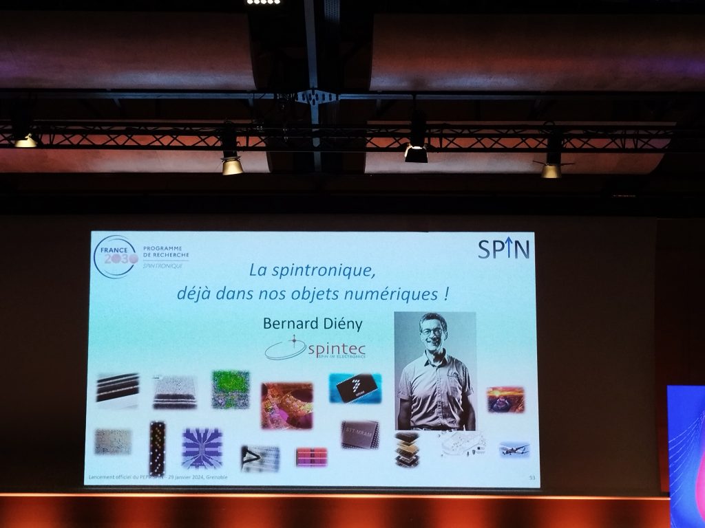
Many prominent researchers from all around France gathered in one place to celebrate the launch but also to share ideas and foster collaboration. The highlight of the day were two very interesting talks. The first one from the 2007 Nobel Laureate for the discovery of the giant magnetoresistance (GMR), Albert Fert about how the field of spintronics has developed over the years and the intriguing future potentials of upcoming phenomena and technologies. The second talk was from the co-founder of Spintec and a well-known name in the world of spintronics especially magnetic random-access memories (MRAMs), Bernard Dieny. He talked about the plethora of applications where magnetism and spintronics could be applied ranging from microelectronics to healthcare. If you are interested in how memory works in a computer and how does spintronics fit into memory technology, check out this post (Link to post).
The talks helped put my own research in perspective to the broader picture. As a student, the next most important thing for me was the food. It helped recover the calories that I spent understanding the talks given in French.
2007 Nobel Laureate Albert Fert talking about Spins!Talk of Spintec co-founder Bernard Dieny about application of spintronics in current technology
In the evening, we were welcomed at the Musée de Grenoble for the gala evening. I got the opportunity to interact with colleagues from different research centers in Grenoble and from different cities of France. I like these events since they allow us to discuss and get acquainted with each other in an informal setting. Sharing their love for science, food and art, hundreds of researchers enjoyed an evening away from experiments, data, and research papers. Although I am sure, there were a lot of scientific discussions that were casually brought in.
Memory Hierarchy – How does computer memory work ?
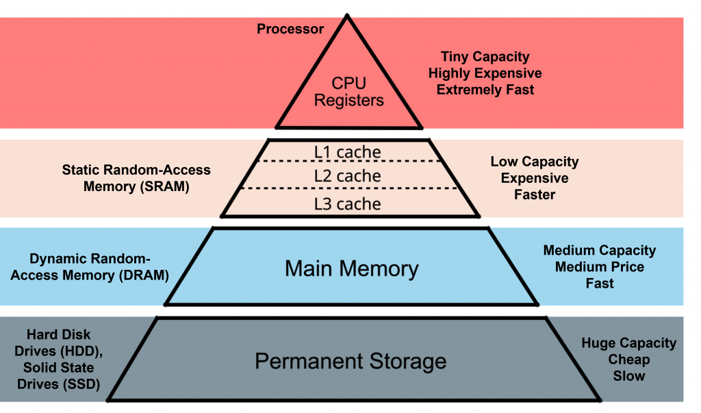
It’s 5pm on a Friday evening. I am done for the week. I save my half-completed article and prepare to leave. A fleeting thought says – “How is my file saved? How is data stored and accessed in a computer?” In this post, I try to answer these questions and understand how memory works in our computers with some examples. The file I saved is broken down into numerous bits or binary digits (0 or 1) and stored in memory units with each memory unit having either 0 or 1. Most computers are structured as a pyramid with the central processing unit (CPU) at the top as shown in figure 1. As we move downwards, we encounter short-term memory for frequently accessed tasks followed by long-term memory for permanent storage. While short-term memory is fast (5000-6000 megabytes per second) and has a smaller capacity (a few gigabytes) [1,2], long-term memory can be huge (a few terabytes) but is extremely slow (around 550 megabytes per second or less) [3]. Let’s take a look at the long-term or storage memories first.
Figure 1:The memory hierarchy or memory pyramid
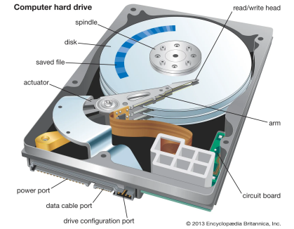
Two broad technologies exist for long-term storage – hard disk drive (HDD) and solid-state drive (SSD). HDD stores data in magnetic domains in layers of magnetic film deposited on a rotating disk as shown in figure 2. Writing and reading is achieved by a read/write head that can read the magnetic state of the domains. This technology was introduced by IBM in 1950s. HDDs are non-volatile and can retain data even after being powered off [3].
Figure 2:Internal structure and components of a hard disk drive. Information is stored in the magnetic state of the magnetic domains and is read or written by the read/write head.
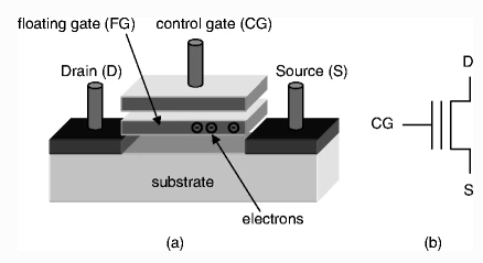
Figure 3:A floating gate transistor which is the basic building block of NAND Flash. A potential applied on the control gate results in transfer of charges from the transistor channel to the floating gate or vice-versa.
SSDs are based on a technology known as NAND Flash [4,5] developed by Fujio Masuoka at Toshiba in 1980s [6]. The basic building block of NAND flash is shown in figure 3. A potential difference between source and drain creates a channel of electron flow between them. Depending on the voltage applied at the control gate on top, some electrons are removed from or trapped in the floating gate. The presence or absence of the electrons results in a change in the resistance state of the device. Millions of such devices are arranged in a crossbar array to manufacture modern SSDs [3,7,8]. SSDs are 10 times faster than HDDs since they do not any mechanically moving parts. Although more expensive than HDDs, SSDs are used where high data transfer speeds and lower delays are desired. In case you haven’t already figured it out, modern thumb drives or flash drives are also based on the NAND flash technology. Most modern laptops and computers use SSDs for permanent storage whereas big data storage farms use a combination of HDDs and SSDs.
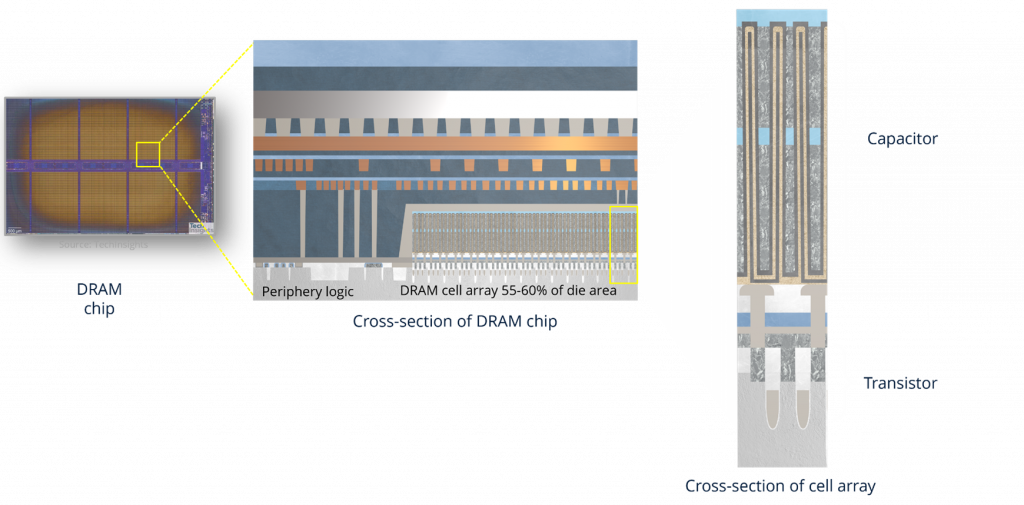
Figure 4:Cross-section of a DRAM chip and its cell array. Periphery logic is used to control the read, write and flow of information to/from the chip. Cross-section of the cell array shows the transistor and the capacitor of the 1T1C structure.
HDDs and SSDs are located at the bottom of the memory pyramid since they have huge memory capacity but slow access speeds. As we move up the pyramid, we come across dynamic random-access memory (DRAM) which is also popularly known as RAM. Also known as the main memory of the computer, DRAM stores the data of currently running programs. As the name random-access suggests, the data at any location in a DRAM can be accessed at any time. It was invented by Robert Dennard at IBM in the 1960s. The basic memory unit in a DRAM consists of a transistor and a capacitor in a 1T1C structure (shown in figure 4). Fully charged and completely empty capacitors denote 1 and 0 respectively. The source of the transistor is connected to the bitline (BL), the drain to the capacitor and the gate is connected to the wordline (WL). If we want to write a 1, the WL is opened, and the transistor is switched on. Electrical charges can now flow from the BL to the capacitor until it is fully charged. The transistor is then turned off and the charge in the capacitor is isolated. However, the charges are not perfectly isolated and leak out over time. The capacitive memory then must be re-written after a certain period [9]. Thousands of these 1T1C structures are arranged in arrays called banks. Multiple banks are combined to form a chip. Multiple parallelly working chips are combined to form the DRAM. DRAM has a capacity of a few gigabytes and access times in 10s of nanoseconds.
Figure 5:An SRAM chip
As we move further up in our memory pyramid, we come across cache memory. Cache memory stores frequently used instructions and data to improve computation time. Cache memory is implemented by a technology called static random-access memory (SRAM) (shown in figure 5). The memory unit of the SRAM is implemented by a combination of six transistors (6T). Since the operation of SRAM does not include the charging and discharging of a capacitor, it is faster than the DRAM. However, 6 transistors in a single memory unit in SRAM increase its cost and reduce the number of memory units that can be squeezed in a given area [10–12]. Cache memory is often referred to as “on-chip memory”.
What happens when I run a game, a software or just open a file?
Imagine I want to play the latest Assassin’s Creed on my computer. The game itself is installed in permanent storage (in the SSDs). When I run the game, the CPU sends around a lot of instructions to control the flow of data. The information is copied from the storage to main memory (to the DRAM). Remember the big “LOADING……” bar at the start? This transfer is necessary to reduce the latency while running the program and the reason behind minimum RAM requirements for all games and software. Depending on what part of the game you are currently playing, a part of the data is copied to the cache memory. Then, a part of that data on the cache is copied to the CPU registers and processed by the CPU. Now, imagine if the memory pyramid doesn’t exist and the CPU is forced to run the program directly from the permanent storage. Since the permanent storage is extremely slow compared to the cache memory, your agile assassin would be moving slower than a tortoise. Here are some videos (Video 1, Video 2) on YouTube that can help you understand more about how memory works in a computer.
How does spintronics come into the picture?
Multiple transfers of data make up most of the energy consumption of a computer. DRAM and SRAM are volatile memories which means once you turn off the power, all their data is lost and their memory needs to be re-written once they are turned on again. Also, as the size of transistors continues to decrease, the energy loss in terms of leakage current increases significantly. Current research is focused on replacing DRAM and SRAM with non-volatile technologies which can store data without the need for continuous power supply and have minimal leakage. One of the most promising solutions is to store data in magnets or magnetic devices. This has led to the development of magnetic random-access memories (MRAM). Spin transfer torque MRAM (STT-MRAM) products from Everspin technologies is already available in the market [13] and can compete with DRAM for certain applications. Meanwhile, spin-orbit torque MRAM (SOT-MRAM) [14,15] continues to garner interest from academia and industry and can potentially compete with SRAM in certain applications. Novel concepts for domain wall [16] and skyrmion-based [17] devices that can find their applications as CPU registers are also under development. While we continue to find solutions to improve our current computing scheme, there are plenty of emerging computing schemes that can overhaul the whole computing landscape. Check those out in previous posts (Maha’s blog, Marco’s blog, Paolo’s blog).
If you found this useful and/or would like to discuss further, don’t hesitate to contact me on LinkedIn.
References
[1] DDR5 | DRAM, https://semiconductor.samsung.com/dram/ddr/ddr5. [2] DDR5 SDRAM Datasheet and Parts Catalog, https://www.micron.com/products/dram/ddr5-sdram/part-catalog. [3] DC600M Enterprise SATA 3.0 SSD – 480GB – 7680GB – Kingston Technology, https://www.kingston.com/en/ssd/dc600m-data-center-solid-state-drive. [4] C. Monzio Compagnoni, A. Goda, A. S. Spinelli, P. Feeley, A. L. Lacaita, and A. Visconti, Reviewing the Evolution of the NAND Flash Technology, Proceedings of the IEEE 105, 1609 (2017). [5] NAND Flash Memory, https://www.micron.com/products/nand-flash. [6] F. Masuoka and H. Iizuka, Semiconductor Memory Device and Method for Manufacturing the Same, US4531203A (23 July 1985). [7] R. Micheloni, A. Marelli, and S. Commodaro, NAND Overview: From Memory to Systems, in Inside NAND Flash Memories, edited by R. Micheloni, L. Crippa, and A. Marelli (Springer Netherlands, Dordrecht, 2010), pp. 19–53. [8] SanDisk Ultra 3D NAND SSD 2.5" 250 GB – 4 TB SATA III Internal SSD, https://www.westerndigital.com/products/internal-drives/sandisk-ultra-3d-sata-iii-ssd.sku=SDSSDH3-500G-G26. [9] S. R. S. Raman, A Review on Non-Volatile and Volatile Emerging Memory Technologies, in Computer Memory and Data Storage (IntechOpen, 2024). [10] SRAMs | Renesas, https://www.renesas.com/us/en/products/memory-logic/srams [11] Synchronous SRAMs, https://www.alliancememory.com/products/synchronous-srams/ [12] A. Pavlov and M. Sachdev, editors , Introduction and Motivation, in CMOS SRAM Circuit Design and Parametric Test in Nano-Scaled Technologies: Process-Aware SRAM Design and Test (Springer Netherlands, Dordrecht, 2008), pp. 1–12. [13] Spin-Transfer Torque DDR Products | Everspin, https://www.everspin.com/spin-transfer-torque-ddr-products. [14] K. Garello et al., Manufacturable 300mm Platform Solution for Field-Free Switching SOT-MRAM, 2 (n.d.). [15] I. Mihai Miron, G. Gaudin, S. Auffret, B. Rodmacq, A. Schuhl, S. Pizzini, J. Vogel, and P. Gambardella, Current-Driven Spin Torque Induced by the Rashba Effect in a Ferromagnetic Metal Layer, Nature Mater 9, 3 (2010). [16] S. S. P. Parkin, M. Hayashi, and L. Thomas, Magnetic Domain-Wall Racetrack Memory, Science 320, 190 (2008). [17] R. Tomasello, E. Martinez, R. Zivieri, L. Torres, M. Carpentieri, and G. Finocchio, A Strategy for the Design of Skyrmion Racetrack Memories, Sci Rep 4, 1 (2014).
The journey of doctoral research is full of excitement and intellectual stimulation. As a doctoral candidate, we spend a lot of time delving into the depths of our research topics, analysing and assimilating new knowledge each day and acquiring new skills that goes on to shape our careers in the future. While our main focus is on working on our research topics and contribute to the advancement of the scientific knowledge, the major aspect of building a professional network is often overlooked. The main reasons for not neglecting professional networking during your PhD are:
1. Expanding your knowledge and perspectives by exchanging ideas with fellow researchers and scholars
2. Identifying potential collaborators and building a framework for joint publications, grants and projects
3. Gaining insights into industry trends, career paths and job opportunities and establishing relationships with experienced professionals for guidance
4. Gaining access to funding opportunities and resources like specialized equipment, facilities and expertise not available at your own institution
5. Enhancing communication and presentation skills
As part of SPEAR, I get to benefit from both industrial and academic networking opportunities. I have gained insights into how an industrial entity functions by sharing my results and exchanging ideas in team meetings and meetings with partners at Antaios. I also try to take advantage of the rich scientific culture in Grenoble. Last month, I had the opportunity to present my work at Rencontres des Jeunes Physicien(ne)s, 2023. Many young physicists from Grenoble presented their work ranging from biophysics to astronomy. It was a fruitful day where we learnt about nature photography and some awe-inspiring photos from the James Webb Telescope.
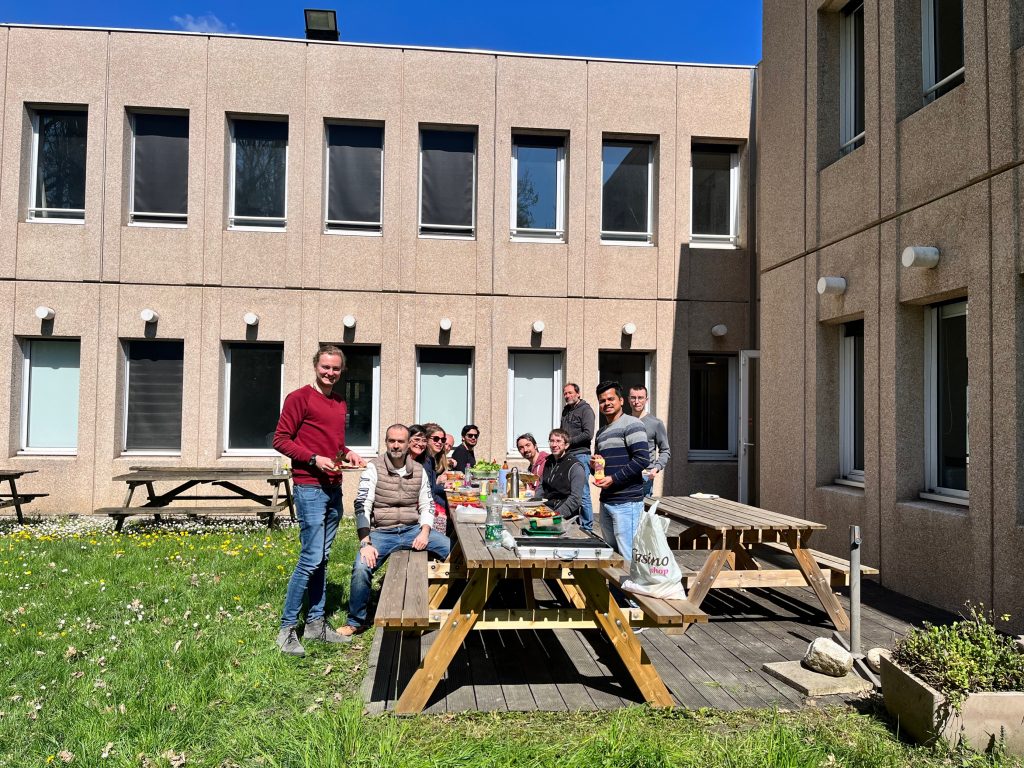
Barbecue Lunch with Antaios family (with Marco, ESR3)
SPEAR training sessions are an excellent opportunity for networking. We not only build strong connections within ourselves but also exchange ideas with the invited speakers who bring a wide range of ideas, experience and technical expertise. We get a chance to develop a collaborative project in a new environment during our secondments. Last few months, we hosted Marco (ESR 3) at Antaios and we had a great time discussing results, exchanging ideas and spending hours in the lab. I am looking forward to my secondment at ETH Zurich for a beautiful Swiss experience and to benefit from their expertise in spin orbit torques.
European School of Magnetism – Two weeks of training, fun and friendships
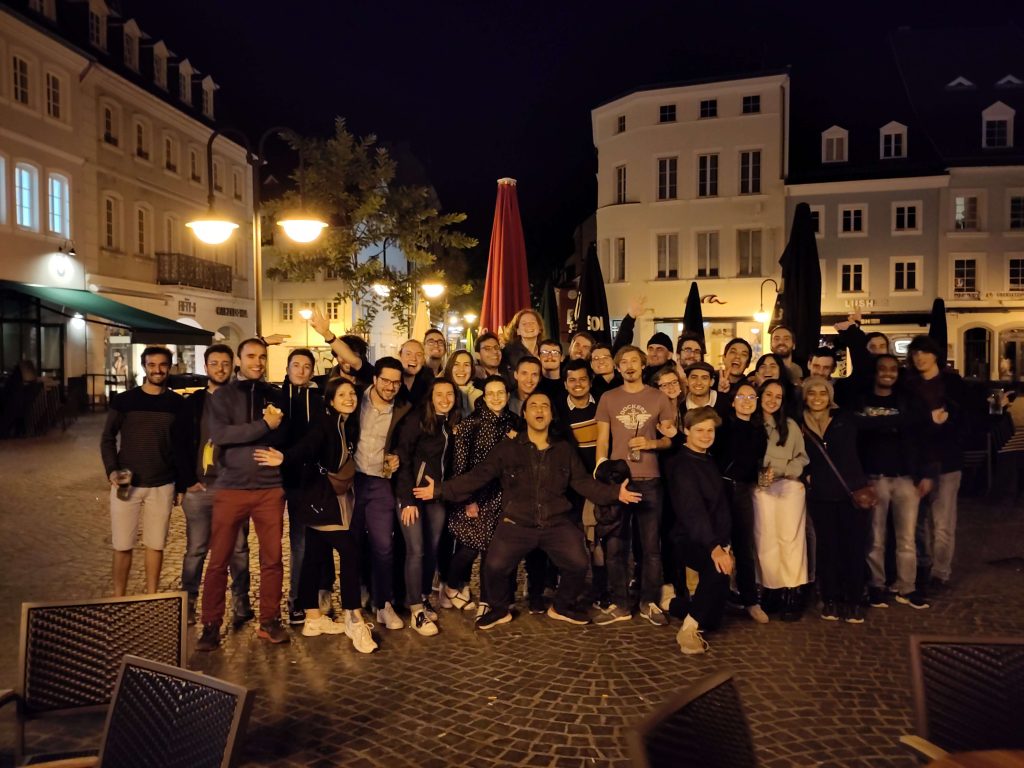
What happens when you take around a hundred students working in the field of magnetism and put them in the same place? You end up with a mix of intriguing ideas, intense discussions, heated sports sessions, and lots of fun. This is how I would describe the two weeks in the mid of September spent in the European School of Magnetism (ESM) in Saarbrucken. It was a nice opportunity to meet new people, form new connections and get together with fellow ESRs (Eoin (ESR1), Marco (ESR3), Salvatore (ESR7), Paolo (ESR8), Sergio (ESR9), Vishesh (ESR11) and Zhewen (ESR13)).
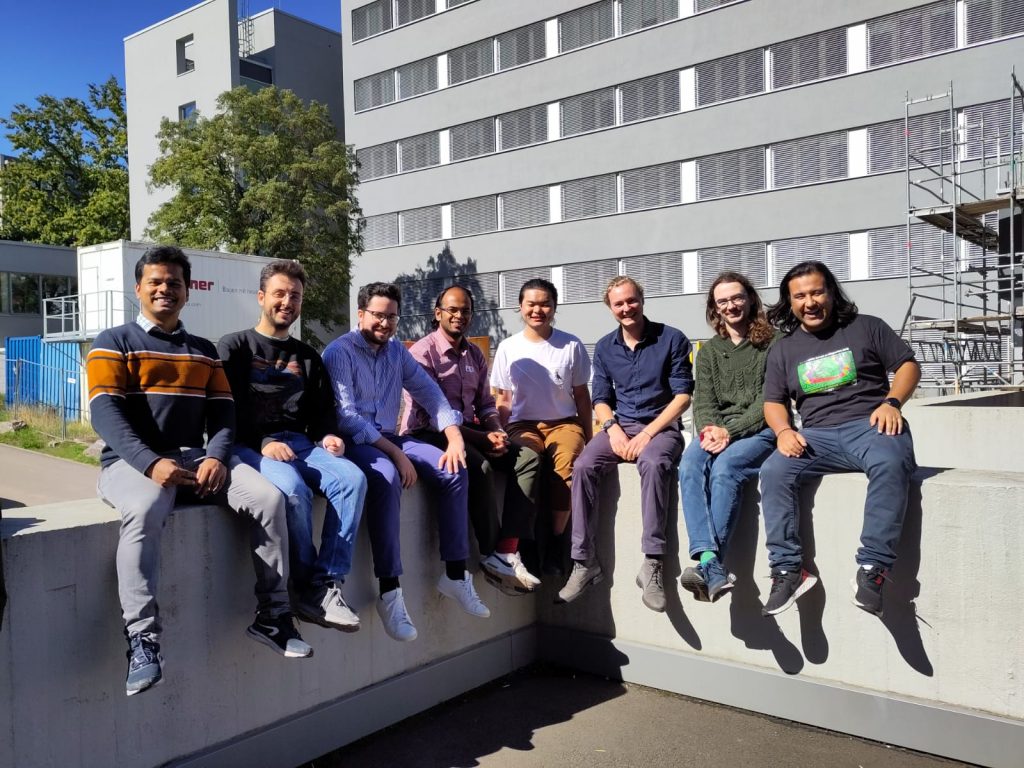
Me (ESR14), Salvatore (ESR7), Paolo (ESR8), Vishesh (ESR11), Zhewen (ESR13), Marco (ESR3), Eoin (ESR1) and Sergio (ESR9) during the European School of Magnetism in Saarbrucken, Germany
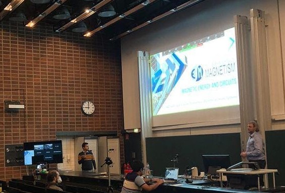
Leading professors and researchers from various fields of magnetism gave lectures on topics ranging from fundamentals of magnetism to applications. I was fascinated by how some properties that we generally take for granted have such complex origins. It was also interesting to learn about the wide variety of magnetic materials (ferromagnetic, antiferromagnetic, ferrimagnetic, multiferroics, magnetocaloric, magnetoelectric, etc) and their wide range of applications. Some lectures were organized to give the participants an industrial perspective on the field of magnetism which were really helpful for people willing to go to the industry or start their own venture. Some volunteers from the participants were also given the opportunity to chair lecture sessions. I also had the opportunity to chair a session by Johannes Paulides on Electric motors and generators.
Chairing a lecture session by Johannes Paulides from Advanced Electromagnetics on electric motors and generators
We also had the opportunity to experience a day of practical experiments in the labs of Technische Universitat of Kaiserslautern and Institut Jean Lamour in Nancy. We were divided into groups and sent to one of the two institutions. My group got the opportunity some broadband ferromagnetic resonance (BB-FMR) measurements at TU Kaiserslautern. It was interesting to carry out experiments outside the scope of my project.
Since the theme for this year was “Basic magnetism for sustainable development”, a crucial element of the school was student projects to solve sustainability issues using magnetism. Along with Marco (ESR3) and other participants, our group tackled the issue of energy efficiency in computation using neuromorphic computing. We presented a range of magnetoelectric, spintronic, and magnonic devices and architectures that can potentially solve this issue. Overall, it was an amazing experience interacting with people from different backgrounds and working on different projects. Surely, the seeds of many potential collaborations and partnerships were sown over the food table, coffee breaks, poster sessions, and late-night discussions, which will reap rewards in the future. In my opinion, if you are working in the field of magnetism, you should attend a session of ESM during your Ph.D.
Last evening of the European School of Magnetism 2022
Grenoble – Convergence of Science, Technology and Nature
It has been a few weeks since I started working at Antaios in Grenoble. Surrounded by the Chartreuse, the Vercors, and the Belledonne mountain chains, Grenoble serves as a gateway to the Alps. These mountain chains act as a directional reference for the people of Grenoble. For example, the doors to our office in Meylan are named after the mountain chains they face, Chartreuse and Belledonne.
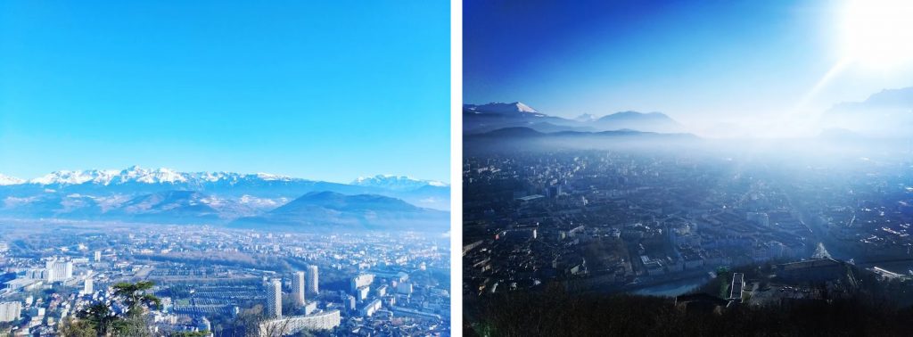
Grenoble is a city full of adventure sports enthusiasts with activities ranging from hiking and rock climbing to skiing and snowboarding. I intend to take full advantage of these opportunities. One of the most common is the hike to the Fort de la Bastille. It is very easy to be enchanted by the bird’s eye view of the city from the top, especially during sunset or sunrise.
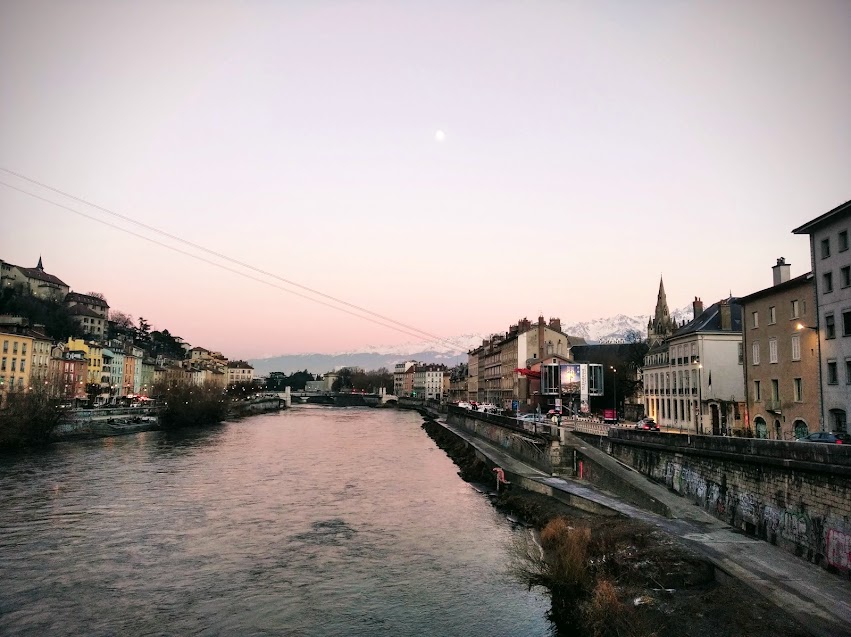
The rivers, Drac and Isére, add to the natural beauty of the city. Positioned at the convergence of these rivers lies the Polygone Scientifique which is home to many research laboratories like Spintec, Institut Néel, and European Synchrotron Radiation Facility (ESRF). I got a chance to visit Spintec and get a glimpse of these reputed research facilities.
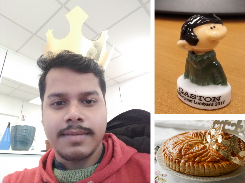
Antaios feels more like a big family than a company to me. My colleagues introduced me to the French tradition of the Galette des Rois. Some of us bring a special cake, called the Galette des Rois, cut into multiple pieces. In one of the cake pieces is a small figurine. If you happen to have it in yours, you are declared the “King of the Day” and then it is your turn to get the Galette des Rois next.
Apart from such traditions, I am currently receiving training on different measurement techniques, simulation software, and design tools. It has been quite an interesting experience working with helpful and experienced colleagues. Everyday brings new knowledge and exciting challenges in the form of training and discussions. I look forward to working and learning with everyone at Antaios.