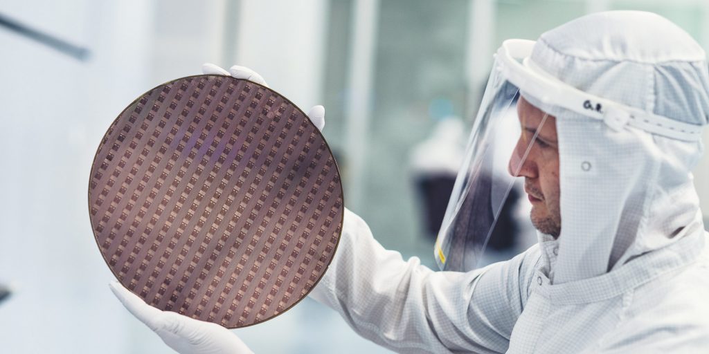
Memory matters!
First, let’s look at the definition of computer memory from Wikipedia, ‘memory is a device or system that is used to store information for immediate use in a computer or related computer hardware and digital electronic devices 1.’ Based on Von Neumann’s architecture, a memory can store many data coded in binary, which are ‘0’ and ‘1’. All information is stored and processed in the form of binary bits. Thanks to memory, your smartphone or laptop can keep up with your endless selfies, streaming, and meme collection.
These days, we demand so much from our devices that the memory inside has to work faster, be more efficient, and somehow use less power. Our iPhones or Androids are crammed with memory chips that now go up to gigabytes or even terabytes, yet our hunger for more memory never seems to be satisfied. Plus, our devices run out of battery way too fast! The MRAM is a magical-sounding memory tech that could solve our tech troubles.

What is MRAM?
Magnetoresistive random-access memory (MRAM) is a promising candidate for next-generation memory, as it is a non-volatile (it doesn’t lose data when powered off), fast-speed, high-density, and energy-efficient memory technology. Figure 1 shows the core of a MRAM cell, magnetic tunnel junction which is a pillar consisting of three layers. They include two ferromagnetic layers separated by one spacer. The magnetization directions of top and bottom ferromagnets are pointed out by arrows. In Figure 1, the magnetization of top layer is fixed, while the bottom free layer’s magnetization can be switched by an external magnetic field or current.

How does MRAM work?
There are a few tricks to this in MRAM. Early MRAM used external magnetic fields to get the job done, but that required a lot of energy (and wasn’t too stable). Luckily, scientists came up with some new ways: spin-transfer torque (STT)2 and spin-orbit torque (SOT)3.
In STT-MRAM, an electric current (green line) passes through the device directly to flip the free magnetic layer. In SOT-MRAM, there’s an extra path for this current, which uses something called the spin Hall effect (fancy physics term alert) to change the magnet direction. Separated write and read lines ensure excellent endurance and the switching time under SOT can be achieved in sub-ns.
While these two methods have their differences, the way MRAM reads data is pretty much the same across the board. MRAM “reads” by measuring the resistance between the two magnetic layers. When the magnets are parallel, the resistance is low — that’s our “0.” When they’re anti-parallel, the resistance is high — a “1.”

The future of MRAM — high density and low power
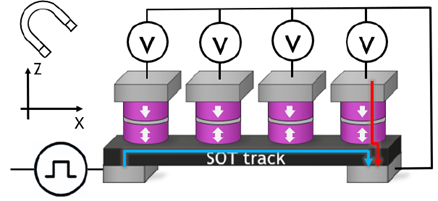
From Figure 3, although the SOT-MRAM has a high endurance benefit from the separated path, it has three terminals resulting in a low integration density. A multi-pillar design was proposed to solve this problem (Figure 4)4. In conventional single-pillar devices, one pillar needs at least two transistors. In multi-pillar devices, the number of required transistors per pillar can be reduced to (1+1/N), where N is the number of pillars. The reduced number of transistors can effectively save space and improve the density of devices.

In principle, the multi-pillar device cannot work without the individual control of each pillar. Because all four pillars will be switched together when we only want to write on a specific cell, leading to a chaos of information. To solve this problem, applying a gate voltage can realize the selective operation in multi-pillar devices. To be specific, a positive gate voltage can lower the energy barrier between the ‘0’ state and ‘1’ state to decrease the critical switching current, while a negative voltage can increase it (Figure 5). On the one hand, during the selective operation, only the pillar under positive gates can be switched. By applying a specific gate voltage on each pillar, we can control which pillar will be written individually. On the other hand, the positive gate voltage can lead to a low working power.

In short, MRAM is not only cool, but it could actually be a game changer for the future of electronics. So, next time you pick up your phone or use your smartwatch, think about all the tiny magnetic switches making it tick.
- https://en.wikipedia.org/wiki/Computer_memory ↩︎
- Ralph, Daniel C., and Mark D. Stiles. “Spin transfer torques.” Journal of Magnetism and Magnetic Materials 320.7 (2008): 1190-1216. ↩︎
- Gambardella, Pietro, and Ioan Mihai Miron. “Current-induced spin–orbit torques.” Philosophical Transactions of the Royal Society A: Mathematical, Physical and Engineering Sciences 369.1948 (2011): 3175-3197. ↩︎
- Cai, K., et al. “Selective operations of multi-pillar SOT-MRAM for high density and low power embedded memories.” 2022 IEEE Symposium on VLSI Technology and Circuits (VLSI Technology and Circuits). IEEE, 2022. ↩︎
Thanks for your reading. The story of MRAM is continuing. If you have questions, feel free to contact me at email: kaiquan.fan@imec.be