In the fascinating world of physics and electronics, the term “spin” of an electron holds a pivotal place. While it might sound like something out of a science fiction movie, the electron’s spin is a fundamental property that has revolutionized our understanding of the microscopic world and paved the way for groundbreaking technologies, particularly in the field of spintronics. This blog post aims to demystify the electron spin and introduce some spintronic devices like the Nobel Prize-winning discovery of Giant Magnetoresistance (GMR), which is responsible for the high storage capacities of modern hard drives. We will also explore some exciting applications and future prospects of spintronics.
While the term “spintronics” may have different connotations for different people, this blog post primarily focuses on providing a brief introduction to this field mainly from the perspective of data storage devices. However, the field expands into other domains, involving the science and technology of using the spin degree of freedom of charge carriers to store, encode, access, process, and transmit information. The field is extremely vast, and discussing everything is beyond the scope of this post.
Interest in spintronics was motivated by a longstanding belief that replacing charge with spin could yield significant advantages in terms of processing speed, energy efficiency, and device density on a chip. These advancements have become an absolute necessity in the 21st century considering the growing demand for energy in the information and communication sector. This demand is expected to consume 20% of global electricity by 2030.

The internet has grown exponentially over the last two decades. To put this into perspective, if the data stored on the internet today were printed on paper, it would form a stack reaching beyond the moon! This massive growth highlights the urgent need for more efficient data storage solutions, where spintronics could play a crucial role.
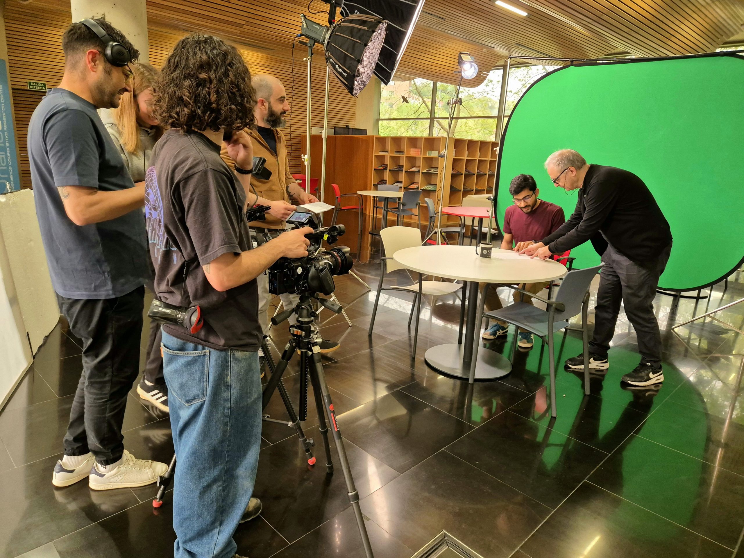
You can also checkout our project video which provides insights on the working principles of spintronics and how it is helping to tranform digital technologies.
What is electron spin?
To grasp the concept of electron spin, it’s essential to understand the basics of atomic structure. Electrons are subatomic particles that, along with protons and neutrons, make up an atom. These elementary particles all possess a quantum mechanical property called spin, which can be measured and has quantized values, including zero.
For the sake of understanding, students often visualize spin as the angular momentum associated with an elementary particle spinning or rotating about its own axis, like a spinning top or a planet. This mental picture is convenient but somewhat crude and incomplete.


There are a few problems with this simplistic picture of an electron’s rotation about its own axis. This model cannot explain the quantization of spin angular momentum, as it suggests that spin should have continuous values rather than discrete ones.
Another problem arises when we try to calculate the spin angular momentum using this semi classical picture.

Where m0 is the mass of electron, vs is the speed of the surface of electron and re is the Lorentz radius of the electron given by,

Solving the above equation, we find that the speed of rotation on the surface of the electron exceeds 130 times the speed of light. Clearly, this would not be permitted by the Einstein’s theory of relativity.
What does this apparent fallacy imply? It indicates that the concept of spin is inherently quantum mechanical and cannot be described within the framework of classical mechanics. Furthermore, the electron cannot be visualized as a nearly point charge with the Lorentz radius.
Landau and Lifshitz, in their classic textbook on quantum mechanics wrote “[the spin] property of elementary particles is peculiar to quantum theory. [It] has no classical interpretation… It would be wholly meaningless to imagine the ‘intrinsic’ angular momentum of an elementary particle as being the result of its rotation about its own axis.”
Experimental and Theoretical Developments
Throughout the 20th century, numerous experiments and theoretical developments significantly enhanced our understanding of the electron’s spin. One of the most pivotal experiments was the Stern-Gerlach experiment in 1922, which demonstrated the quantized nature of angular momentum and provided direct evidence of spin. In this experiment, silver atoms were passed through a non-uniform magnetic field, resulting in the atoms being deflected in discrete directions rather than a continuous spread, indicating the presence of quantized spin states.

Further theoretical advancements came with the development of quantum mechanics. Paul Dirac’s relativistic quantum theory in 1928 successfully incorporated spin into the framework of quantum mechanics, predicting the existence of antimatter and providing a more comprehensive understanding of the electron’s behaviour.
Experimental techniques continued to evolve, allowing more precise measurements of spin-related phenomena. For instance, the discovery of electron spin resonance (ESR) in 1944 enabled scientists to study the magnetic properties of electrons in various materials. This technique exploits the fact that electron spins can resonate in an external magnetic field, providing detailed information about the electronic structure of substances.
Another significant milestone was the development of the scanning tunneling microscope (STM) in the 1980s, which allowed for the visualization and manipulation of individual atoms and their spins on surfaces. This breakthrough opened new avenues for research in surface physics and nanotechnology.
These theoretical and experimental advances have collectively deepened our understanding of spin and its behaviour under different conditions. They have paved the way for modern applications in fields such as spintronics, where the manipulation of the electron’s spin is used to develop new technologies for data storage and processing. The interplay between theory and experiment continues to drive progress in understanding the fundamental properties of matter.
Spintronics: Electronics with electron spin
In the mid-20th century, it became clear that electron spin plays a fundamental role in magnetism. Every theoretical model developed to explain the physical origins of magnetism, such as the Bloch model, the Heisenberg model, and the Stoner model, invoked spin in some way.
While magnetism has always been closely linked with spin, in the late 20th century came a breakthrough realization: spin, either alone or in conjunction with charge, can be harnessed to process information. An electron can have one of two spin states: “spin-up” or “spin-down,” typically represented by arrows pointing up or down. This binary nature of spin makes it an excellent candidate for encoding information, similar to how binary code (0s and 1s) is used in traditional computing.

This role had been traditionally delegated to the “charge” of an electron, not its “spin.” Over the last two decades or so, there has been burgeoning interest in augmenting the role of charge with spin, or even replacing charge with spin in information processing devices.

Giant Magnetoresistance
The discovery of GMR was a groundbreaking moment in the field of spintronics and in physics, achieved independently by Albert Fert in France and Peter Grünberg in Germany in 1988. Their work demonstrated how the resistance of multilayered magnetic structures could change dramatically in response to an external magnetic field. This discovery was so impactful that it earned them the Nobel Prize in Physics in 2007.
GMR is a quantum mechanical magnetoresistance effect observed in thin film structures composed of alternating ferromagnetic and non-magnetic layers. The resistance of these structures changes significantly in response to an external magnetic field.
Working principle of GMR
Layer Structure: The GMR effect is typically observed in multilayered structures where layers of ferromagnetic materials (like iron or cobalt) are separated by a non-magnetic spacer layer (such as chromium or copper).
Spin-Dependent Scattering: Electrons in ferromagnetic materials have spins that can be either parallel or antiparallel to the magnetization of the layers. The resistance of the material depends on the relative orientation of these spins.
Parallel Alignment: When the magnetizations of the two ferromagnetic layers are parallel, electrons encounter less scattering (i.e. current flowing through the layers will encounter lower resistance).
Antiparallel Alignment: When the magnetizations are antiparallel, the scattering increases (i.e. current flowing through the layers will encounter lower resistance).
Magnetic Field Influence: The magnetization of one of the ferromagnetic layers can be switched at will by applying a magnetic field. This change in resistance of the structure depending on the magnetization state of two ferromagnetic layers is the GMR effect, and it allows external control of the resistance state (high/low) of the structure.

Right schematic (adapted ref. 6): GMR sensor reading individual bits
Applications of GMR
-Hard Disk Drives (HDDs): GMR read heads are used in modern HDDs. The ability to detect small changes in magnetic fields allows for the reading of densely packed data on the disk, significantly increasing storage capacity leading to HDDs with terabyte-level capacities
– Magnetic Field Sensors: GMR sensors are used in various applications to detect magnetic fields with high sensitivity. These sensors are used in automotive applications, industrial positioning, and consumer electronics.
– Biological and Chemical Sensors: GMR-based sensors are being developed for detecting biomolecules and chemical substances, taking advantage of their high sensitivity and specificity.
Giant Magnetoresistance and spin valves have not only advanced data storage technology but also opened new frontiers in sensor technology and spintronics. Their ability to manipulate and detect electron spin with high precision underscores their significance in both scientific research and practical applications. The continued development and application of GMR technology promise to drive further innovations in electronics and information technology.
Outlook
Looking forward, the field of spintronics holds immense promise for revolutionizing the next generation of electronic devices. Spin Transfer Torque Magnetic RAM (STT-MRAM) and Spin-Orbit Torque RAM (SOT-RAM) are emerging as potential replacements for traditional memory technologies, offering faster speeds, higher endurance, and lower power consumption. Beyond memory, spintronics is paving the way for innovative devices like the MESO (Magnetoelectric Spin-Orbit) device, which could lead to even more energy-efficient computing. These technologies are not just theoretical; they are actively being developed and hold the potential to transform everything from data storage to processing, enabling smarter, faster, and more sustainable electronic systems. The future of spintronics is bright, with the potential to push the boundaries of what’s possible in the digital age.

References:
- Jones, N. (2018). How to stop data centres from gobbling up the world’s electricity. Nature, 561(7722), 163–166. https://doi.org/10.1038/D41586-018-06610-Y
- Bandyopadhyay, S. ., & Cahay, M. . (2020). Introduction to spintronics. CRC Press. https://www.routledge.com/Introduction-to-Spintronics/Bandyopadhyay-Cahay/p/book/9780367656447
- Castelvecchi, D. (2022). The Stern–Gerlach experiment at 100. Nature Reviews Physics 2022 4:3, 4(3), 140–142. https://doi.org/10.1038/s42254-022-00436-4
- How the Stern–Gerlach experiment made physicists believe in quantum mechanics – Physics World. (n.d.). https://physicsworld.com/a/how-the-stern-gerlach-experiment-made-physicists-believe-in-quantum-mechanics/
- Application of GMR | Evgeny Tsymbal | Nebraska. (n.d.). Retrieved August 21, 2024, from https://unlcms.unl.edu/cas/physics/tsymbal/reference/giant_magnetoresistance/application_%20of_gmr.shtml
- CALAVALLE, F., & CALAVALLE, F. (2022). Probing and tuning the electronic properties of low dimensional van der Waals materials. Ph.D thesis UNIVERSIDAD DEL PAÍS VASCO/EUSKAL HERRIKO UNIBERTSITATEA
- Manipatruni, S., Nikonov, D. E., Lin, C. C., Gosavi, T. A., Liu, H., Prasad, B., Huang, Y. L., Bonturim, E., Ramesh, R., & Young, I. A. (2018). Scalable energy-efficient magnetoelectric spin–orbit logic. Nature 2018 565:7737, 565(7737), 35–42. https://doi.org/10.1038/s41586-018-0770-2

