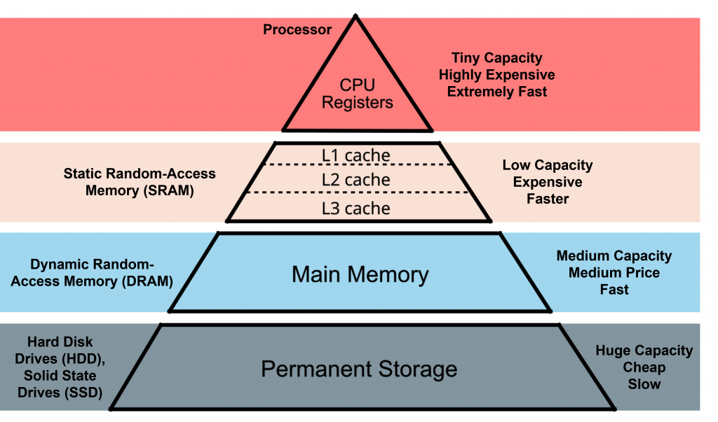
It’s 5pm on a Friday evening. I am done for the week. I save my half-completed article and prepare to leave. A fleeting thought says – “How is my file saved? How is data stored and accessed in a computer?” In this post, I try to answer these questions and understand how memory works in our computers with some examples. The file I saved is broken down into numerous bits or binary digits (0 or 1) and stored in memory units with each memory unit having either 0 or 1. Most computers are structured as a pyramid with the central processing unit (CPU) at the top as shown in figure 1. As we move downwards, we encounter short-term memory for frequently accessed tasks followed by long-term memory for permanent storage. While short-term memory is fast (5000-6000 megabytes per second) and has a smaller capacity (a few gigabytes) [1,2], long-term memory can be huge (a few terabytes) but is extremely slow (around 550 megabytes per second or less) [3]. Let’s take a look at the long-term or storage memories first.
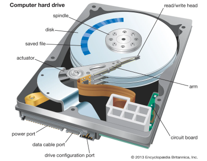
Two broad technologies exist for long-term storage – hard disk drive (HDD) and solid-state drive (SSD). HDD stores data in magnetic domains in layers of magnetic film deposited on a rotating disk as shown in figure 2. Writing and reading is achieved by a read/write head that can read the magnetic state of the domains. This technology was introduced by IBM in 1950s. HDDs are non-volatile and can retain data even after being powered off [3].
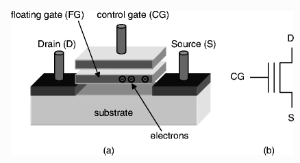
SSDs are based on a technology known as NAND Flash [4,5] developed by Fujio Masuoka at Toshiba in 1980s [6]. The basic building block of NAND flash is shown in figure 3. A potential difference between source and drain creates a channel of electron flow between them. Depending on the voltage applied at the control gate on top, some electrons are removed from or trapped in the floating gate. The presence or absence of the electrons results in a change in the resistance state of the device. Millions of such devices are arranged in a crossbar array to manufacture modern SSDs [3,7,8]. SSDs are 10 times faster than HDDs since they do not any mechanically moving parts. Although more expensive than HDDs, SSDs are used where high data transfer speeds and lower delays are desired. In case you haven’t already figured it out, modern thumb drives or flash drives are also based on the NAND flash technology. Most modern laptops and computers use SSDs for permanent storage whereas big data storage farms use a combination of HDDs and SSDs.
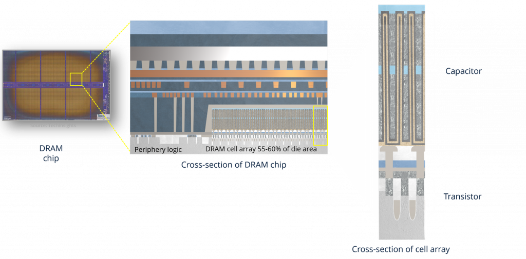
HDDs and SSDs are located at the bottom of the memory pyramid since they have huge memory capacity but slow access speeds. As we move up the pyramid, we come across dynamic random-access memory (DRAM) which is also popularly known as RAM. Also known as the main memory of the computer, DRAM stores the data of currently running programs. As the name random-access suggests, the data at any location in a DRAM can be accessed at any time. It was invented by Robert Dennard at IBM in the 1960s. The basic memory unit in a DRAM consists of a transistor and a capacitor in a 1T1C structure (shown in figure 4). Fully charged and completely empty capacitors denote 1 and 0 respectively. The source of the transistor is connected to the bitline (BL), the drain to the capacitor and the gate is connected to the wordline (WL). If we want to write a 1, the WL is opened, and the transistor is switched on. Electrical charges can now flow from the BL to the capacitor until it is fully charged. The transistor is then turned off and the charge in the capacitor is isolated. However, the charges are not perfectly isolated and leak out over time. The capacitive memory then must be re-written after a certain period [9]. Thousands of these 1T1C structures are arranged in arrays called banks. Multiple banks are combined to form a chip. Multiple parallelly working chips are combined to form the DRAM. DRAM has a capacity of a few gigabytes and access times in 10s of nanoseconds.
As we move further up in our memory pyramid, we come across cache memory. Cache memory stores frequently used instructions and data to improve computation time. Cache memory is implemented by a technology called static random-access memory (SRAM) (shown in figure 5). The memory unit of the SRAM is implemented by a combination of six transistors (6T). Since the operation of SRAM does not include the charging and discharging of a capacitor, it is faster than the DRAM. However, 6 transistors in a single memory unit in SRAM increase its cost and reduce the number of memory units that can be squeezed in a given area [10–12]. Cache memory is often referred to as “on-chip memory”.
What happens when I run a game, a software or just open a file?
Imagine I want to play the latest Assassin’s Creed on my computer. The game itself is installed in permanent storage (in the SSDs). When I run the game, the CPU sends around a lot of instructions to control the flow of data. The information is copied from the storage to main memory (to the DRAM). Remember the big “LOADING……” bar at the start? This transfer is necessary to reduce the latency while running the program and the reason behind minimum RAM requirements for all games and software. Depending on what part of the game you are currently playing, a part of the data is copied to the cache memory. Then, a part of that data on the cache is copied to the CPU registers and processed by the CPU. Now, imagine if the memory pyramid doesn’t exist and the CPU is forced to run the program directly from the permanent storage. Since the permanent storage is extremely slow compared to the cache memory, your agile assassin would be moving slower than a tortoise. Here are some videos (Video 1, Video 2) on YouTube that can help you understand more about how memory works in a computer.
How does spintronics come into the picture?
Multiple transfers of data make up most of the energy consumption of a computer. DRAM and SRAM are volatile memories which means once you turn off the power, all their data is lost and their memory needs to be re-written once they are turned on again. Also, as the size of transistors continues to decrease, the energy loss in terms of leakage current increases significantly. Current research is focused on replacing DRAM and SRAM with non-volatile technologies which can store data without the need for continuous power supply and have minimal leakage. One of the most promising solutions is to store data in magnets or magnetic devices. This has led to the development of magnetic random-access memories (MRAM). Spin transfer torque MRAM (STT-MRAM) products from Everspin technologies is already available in the market [13] and can compete with DRAM for certain applications. Meanwhile, spin-orbit torque MRAM (SOT-MRAM) [14,15] continues to garner interest from academia and industry and can potentially compete with SRAM in certain applications. Novel concepts for domain wall [16] and skyrmion-based [17] devices that can find their applications as CPU registers are also under development. While we continue to find solutions to improve our current computing scheme, there are plenty of emerging computing schemes that can overhaul the whole computing landscape. Check those out in previous posts (Maha’s blog, Marco’s blog, Paolo’s blog).
If you found this useful and/or would like to discuss further, don’t hesitate to contact me on LinkedIn.
References
[1] DDR5 | DRAM, https://semiconductor.samsung.com/dram/ddr/ddr5.
[2] DDR5 SDRAM Datasheet and Parts Catalog, https://www.micron.com/products/dram/ddr5-sdram/part-catalog.
[3] DC600M Enterprise SATA 3.0 SSD – 480GB – 7680GB – Kingston Technology, https://www.kingston.com/en/ssd/dc600m-data-center-solid-state-drive.
[4] C. Monzio Compagnoni, A. Goda, A. S. Spinelli, P. Feeley, A. L. Lacaita, and A. Visconti, Reviewing the Evolution of the NAND Flash Technology, Proceedings of the IEEE 105, 1609 (2017).
[5] NAND Flash Memory, https://www.micron.com/products/nand-flash.
[6] F. Masuoka and H. Iizuka, Semiconductor Memory Device and Method for Manufacturing the Same, US4531203A (23 July 1985).
[7] R. Micheloni, A. Marelli, and S. Commodaro, NAND Overview: From Memory to Systems, in Inside NAND Flash Memories, edited by R. Micheloni, L. Crippa, and A. Marelli (Springer Netherlands, Dordrecht, 2010), pp. 19–53.
[8] SanDisk Ultra 3D NAND SSD 2.5" 250 GB – 4 TB SATA III Internal SSD, https://www.westerndigital.com/products/internal-drives/sandisk-ultra-3d-sata-iii-ssd.sku=SDSSDH3-500G-G26.
[9] S. R. S. Raman, A Review on Non-Volatile and Volatile Emerging Memory Technologies, in Computer Memory and Data Storage (IntechOpen, 2024).
[10] SRAMs | Renesas, https://www.renesas.com/us/en/products/memory-logic/srams
[11] Synchronous SRAMs, https://www.alliancememory.com/products/synchronous-srams/
[12] A. Pavlov and M. Sachdev, editors , Introduction and Motivation, in CMOS SRAM Circuit Design and Parametric Test in Nano-Scaled Technologies: Process-Aware SRAM Design and Test (Springer Netherlands, Dordrecht, 2008), pp. 1–12.
[13] Spin-Transfer Torque DDR Products | Everspin, https://www.everspin.com/spin-transfer-torque-ddr-products.
[14] K. Garello et al., Manufacturable 300mm Platform Solution for Field-Free Switching SOT-MRAM, 2 (n.d.).
[15] I. Mihai Miron, G. Gaudin, S. Auffret, B. Rodmacq, A. Schuhl, S. Pizzini, J. Vogel, and P. Gambardella, Current-Driven Spin Torque Induced by the Rashba Effect in a Ferromagnetic Metal Layer, Nature Mater 9, 3 (2010).
[16] S. S. P. Parkin, M. Hayashi, and L. Thomas, Magnetic Domain-Wall Racetrack Memory, Science 320, 190 (2008).
[17] R. Tomasello, E. Martinez, R. Zivieri, L. Torres, M. Carpentieri, and G. Finocchio, A Strategy for the Design of Skyrmion Racetrack Memories, Sci Rep 4, 1 (2014).
