It all makes me wonder whether anyone has been reading along with me, refreshing the page, anxiously anticipating the next installment, or if I’ve been screaming into the void this entire time?
Making graphene is a critical part of any graphene based project, like mine. But how do we make it? Actually its much easier than one might expect – during lab outreach events we’ve had children with no training whatsoever make perfectly presentable pieces, a fact that really calls into question the value of my two master’s degrees.
The first step in creating graphene involves using scientific-grade adhesive tape to peel a thin layer from a larger piece of graphite, a material composed entirely of carbon atoms arranged in a layered structure. Graphite is similar to the “lead” found in pencils, but in this process, we are interested in isolating its single-layer form, known as graphene. The tape serves as a tool to cleave the graphite, capturing the topmost layers.
Next, the adhesive side of the tape, now holding thin graphite flakes, is pressed firmly onto a meticulously cleaned silicon wafer. Silicon is chosen because its properties enhance graphene visibility under certain lighting conditions, as well as being a convenient surface to do further work on the graphene. The wafer is then heated to improve adhesion, ensuring that some graphite flakes stick properly to its surface. After allowing sufficient time for this process, the tape is slowly and carefully peeled away. This peeling leaves behind an uneven distribution of graphene flakes on the silicon wafer, with pieces varying in size and thickness.
To locate a suitable piece of graphene, we turn to an optical microscope. This instrument allows us to inspect the wafer’s surface with precision. Graphene interacts uniquely with visible light, absorbing it efficiently, which causes it to appear darker than the surrounding silicon. This optical contrast makes it possible to differentiate between flakes of varying thickness. By observing how dark each flake looks, we can estimate the number of graphene layers present, ultimately selecting the desired single-layer graphene for further experimentation.
On the similarities of chip design and the icing of cakes
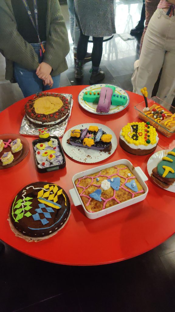
I recently had the opportunity to present my research project in the form of a cake thanks to the PhD workshop at Nanogune. The humble poster is a tried-and-true method for relaying research output, but the cake is an underappreciated medium for the same. A great deal of information can be conveyed with the skillful application of icing, and the careful implantation of chocolate chip impurities in the amorphous sponge matrix. Pictured here (centre cake) is my research project, in icing. The graphene, a honeycomb of black icing balls, the gold contacts, a honey-coloured sheet of icing, and the silicon wafer a honey flavoured layer of nanometre thin sugar. Cooking and explaining my project like this was a surprisingly fun idea, and a creative way to convey information and have a tasty snack.
It makes one think that fabricating chips, something I also do on occasion, is much like baking a cake. In both cases you follow a certain recipe, carefully mix the ingredients, and bake at 1200C for 8-12 hours. In the end you emerge with something round and tasty, and that’s when the fun really begins! An icing of sugar or elemental gold, to really make your work shine. All that’s left is to carefully cut it up and share among friends and collaborators.
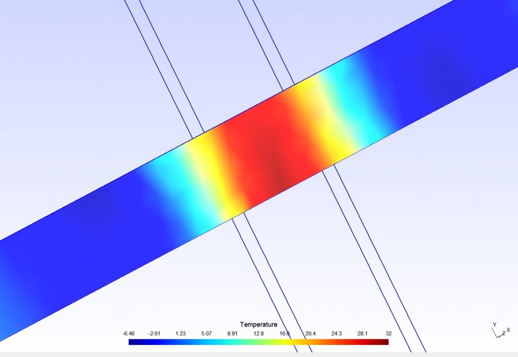
Recently I’ve been taking a small part-time break from my lab activities to engage in something slightly more theoretical, as I use finite element simulations to study what’s really going on with the spin currents in my graphene samples. Finite element analysis (FEA) is a type of numerical simulation that allows one to study complex behaviour in systems which would be very difficult to either explore analytically or visualise intuitively.
There is true beauty in the emergence of complex behaviour from a small number of simple governing equations, and this has helped me gain a greater understanding of my systems and given me several interesting experimental ideas that might never have occurred to me otherwise.
On top of anything else the outputs are quite aesthetically pleasing, pictured is a piece of cold graphene brought into contact with a standard summer day in Donosti. It heats up in a pleasantly Poissonic manner.
As a small side bonus since the only equipment needed is a computer, I’ve gotten some breaks from the lab and had some enjoyable mornings working from places with air conditioning as I hide from San Sebastian’s sibilant summer sizzle. I look forward to the imminent arrival of ESR8 and ESR9, perhaps we will discuss science on the beach if we find the time and sand space.
Learning about spin orbit torques in Leuven and also having fun in Leuven. Leuven, Belgium, 2022
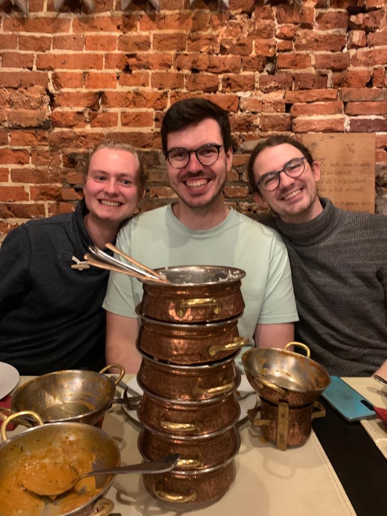
We recently had the wonderful opportunity to learn about spin orbit torque technology at IMEC, a world-leading R&D and innovation hub in nanoelectronics and digital technologies in Leuven, Belgium. During our time there we had a series of enlightening spin orbit talks, giving us a great overview of the current state of the technology in terms of real world applications as well as some more fundamental considerations. We also got the chance to tour the cleanroom facility at IMEC, which is a genuinely impressive construct although unfortunately we’re not allowed to share pictures of it on the blog. As well as the scientific content we also did a series of classes on how to improve our scientific communication skills (although blog posts, alas, were not specifically covered). This was a great opportunity to improve not only our communication skills but to hear about the scientific exploits of the other ESRs. Although learning obviously occupied most of the trip, we did find time for a brief interlude of socialisation during which ESR4 ate an amusingly large amount of rice. Look at that stack of dishes! Classic ESR4, never change.
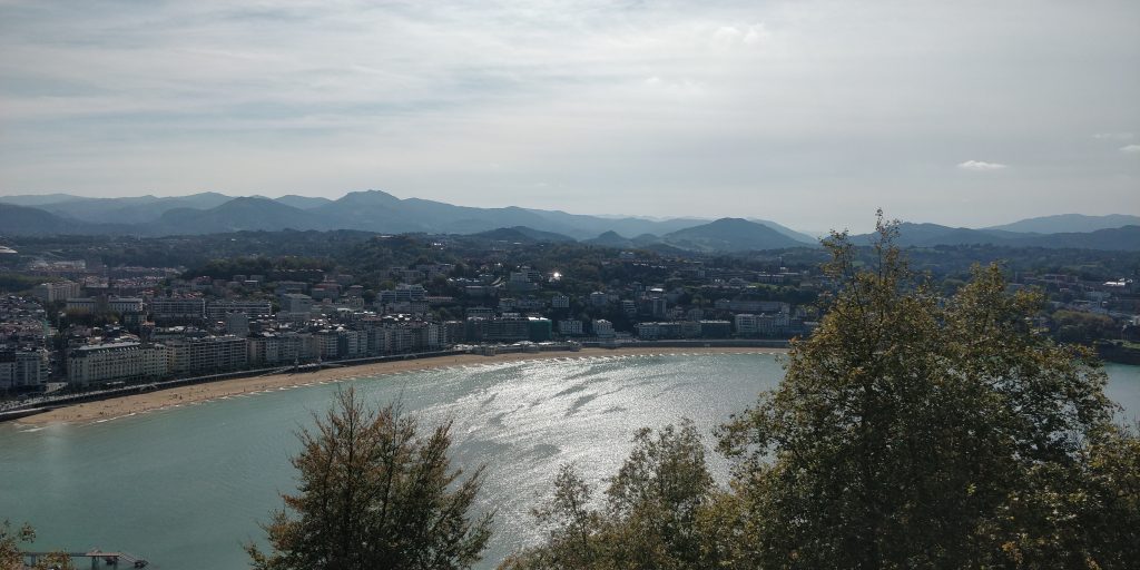
It’s been almost five months now since I moved to San Sebastian, which is rather hard to believe. The city is known around Europe for its rich history, proud food culture, and incredible beaches. Having lived here for a few months now I can certainly see why this is the case. I’m doing my best to learn the language while I’m here, so that I can better appreciate the life here. This has been a really fun challenge, and I think I’m making good progress. Aside from the cultural aspect, the city is also home to a lot of cutting-edge research which I have been lucky enough to be a part of. Here at Nanogune some of the world’s leading work in Spintronics is being carried out. So far, Ive only really started to learn everything, from the theory to the practical techniques needed for this kind of science, so it’s a lot to take in. So far things are going well, and I’m looking forward to continuing my work here.