From Electronics to Spintronics… and Now, Orbitronics?!
The history of information technology is deeply tied to how we manipulate one of the fundamental parts of the atom: the electron. Early on, engineers learned to move the electron’s negative charge through materials, which was used to create electrical currents and store energy through charge accumulation. This control over electrons became the foundation of most devices we use today. (Here, “electronics” comes from “electron,” and “electrical current” means electrons moving together.)
Later, exploiting another property of electrons — their spin — led to new advances. (For a deeper dive into the history and details of spintronics, see Mayank’s excellent post.) The spin of electrons is a complex concept. Still, macroscopically, it can be thought of as an intrinsic identity of the electron, like a color (red or blue) or an arrow (up or down). It gives rise to a tiny magnetic field per electron. By learning to control the spin, we opened the door to a new field called spintronics, where devices manipulate spin currents (electrons with a particular spin moving together) and spin accumulation (electrons with a specific spin gathering in one place).
Of course, this is only a small part of the whole story. The spin is not the only property we can exploit. From the fundamentals of quantum mechanics, we know that an electron’s total angular momentum combines spin and orbital angular momentum — the latter arising from the complex, cloud-like paths that electrons trace as they move along the system and around the centers of atoms. These orbital motions create an additional magnetic moment, meaning electrons can carry magnetism from their spin and orbital motion.” This leads us to a second new set of names: orbitronics, orbital currents, and orbital accumulation.
We can imagine an orbital current as a collective movement of electrons that rotate similarly as they move through a crystal (see the video above). However, detecting orbital accumulation — where orbital angular momentum builds up at material edges — is not as straightforward. It remains a topic of active discussion within the scientific community. For instance, during the recent SPEAR conference (Spin and Orbit in San Sebastián), leading researchers gathered to discuss the state of the art in orbitronics and the major experimental and theoretical challenges ahead.
If spintronics opens the door to new ways of using electrons, then orbitronics opens an additional window to even greater possibilities. Spintronics and orbitronics are deeply intertwined, so separating the effects of spin and orbital currents in many experiments is exceptionally challenging.
This is where my own research comes in.
I study charge-to-spin and orbital conversion — how an incoming electrical current can be transformed into spin and orbital currents. They have to be produced somehow by answering key questions — how, why, how much, and under what conditions — we can identify promising materials that maximize useful effects while minimizing cost and complexity.
Physics is endlessly fascinating on its own, but at some point, our work must also aim toward practical goals: making future devices faster, cheaper, more energy-efficient, and more environmentally friendly.
Despite the current uncertainties, the future of orbitronics is bright. Mastering the orbital degree of freedom is part of a much larger trend: learning to control the hidden properties of electrons and materials.
Under the growing umbrella of “X-Tronics,” fields like: – Valleytronics (controlling electrons based on energy valleys), – Twistronics (tuning properties by twisting atomic layers), – Phononics (managing atomic vibrations),
are rapidly expanding.
The next technological revolution might not be about moving more electrons — but about moving them smarter and more efficiently.
Have you ever wondered how your brain effortlessly recognizes faces, understands language, makes quick decisions, or learns from past experiences? These seemingly simple tasks pose significant challenges for conventional computers, which consume considerable energy handling precise numerical calculations step-by-step. The brain’s remarkable efficiency arises from its ability to perform numerous parallel computations simultaneously, often with lower precision. This observation raises an intriguing question: Can artificial systems replicate the brain’s impressive efficiency?
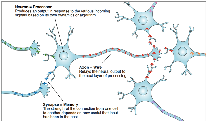
Neuromorphic computing tackles exactly this challenge. This emerging technology aims to mimic the brain’s structure and function, specifically its essential components—neurons and synapses. Neurons are tiny processing units interconnected by synapses that transmit electrical signals known as spikes. Remarkably, the human brain accomplishes all these tasks while consuming only about 20 watts of energy—comparable to a dim light bulb—demonstrating exceptional efficiency. By replicating these biological interactions, neuromorphic computing promises substantial improvements in computational power and energy efficiency, potentially leading to powerful yet sustainable solutions.
One promising technology for neuromorphic computing is spintronics, which utilizes the magnetic spins of electrons to build innovative devices. There are several ways to use spintronic devices for neuromorphic computing. I will talk about my favorite: magnetic skyrmions! Imagine a skyrmion as a tiny magnetic vortex, where electron spins align into stable, swirling patterns resembling miniature whirlpools or galaxies, but in a magnetic material. This intricate configuration gives skyrmions remarkable stability, allowing them to be reliably manipulated by electrical currents at nanoscale dimensions (see figure for a visual example).
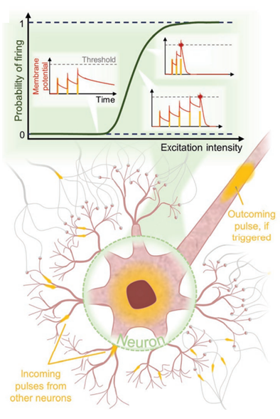
Biological neurons can be effectively modeled using RC circuits—basic electronic components combining resistance (R) and capacitance (C) to control electrical signals. These circuits capture the essential dynamics of neurons through the Leaky-Integrate-Fire (LIF) model, which is widely adopted in neuroscience to describe neuron behavior. Remarkably, skyrmions can replicate these neuronal dynamics at a nanoscale. By placing a skyrmion within a specially engineered magnetic environment where the perpendicular magnetic anisotropy (PMA)—which defines how strongly spins prefer aligning perpendicular to the surface—varies quadratically, the skyrmion moves predictably under electrical stimulation. The applied current induces a force that competes with the force due to the gradient, causing the skyrmion to shift its position, similar to how voltage accumulates in a capacitor during charging. Once the current ceases, the skyrmion naturally returns to its original position, effectively simulating the discharge phase of a capacitor. This motion directly mirrors the LIF neuron’s behavior, which shows that skyrmions have the potential to efficiently emulate biological neuron dynamics.
Scaling these skyrmion-based neuromorphic devices involves overcoming challenges in precise fabrication, maintaining stability, and integrating them into existing technologies. Despite these challenges, skyrmions might have a crucial role in neuromorphic computing. So, can we emulate the brain? Well, at least NOT YET :((. However, scientists have been able to emulate individual neurons with skyrmions (and other spintronic devices). Given that the brain consists of billions upon billions of interconnected neurons, I guess we could say, “Let’s take one neuron at a time… one neuron at a time.”
Van der Waals Heterostructures: From Bulk Crystals to Devices
Materials science has made leaps in recent decades, particularly with the discovery and manipulation of two-dimensional (2D) materials—ultrathin sheets of atoms with unique electronic and magnetic properties. Everything began with the discovery of graphene in 2004, a single layer of carbon atoms with exceptional electrical and mechanical properties. Researchers in Manchester were able to separate a single layer of carbon from its bulk crystal using household sticky tape.
Building on this discovery, researchers began exploring other 2D materials, broadening the possibilities of material science. In the beginning, only a handful of materials were known and used for research. In addition to metallic graphene and insulating hexagonal boron nitride (hBN), more and more materials have been discovered, including magnetic materials, semimetals, and superconductors.
By stacking different 2D materials on top of each other, scientists can create van der Waals heterostructures. These engineered materials offer unprecedented control over electronic and optical properties, leading to significant advancements in electronics, quantum computing, and spintronics., named after the weak interlayer forces that hold them together. These structures allow researchers to tailor new materials with properties that do not exist in nature, leading to advancements in electronics, quantum computing, and spintronics. While the initial methods for creating artificial crystals were highly complex and had limited success, this changed with the introduction of the PDMS-PC dry stacking technique. A device that was created using this technique is shown in Fig. 1. The bulk material images were taken from the website of the Quantum Materials Lab of the University of Arkansas which provides a great overview of exfoliatable materials.
Fig. 1 Comparison of bulk crystals and artificial heterostructures created from exfoliated flakes of these materials.
Before constructing these heterostructures, researchers must first prepare the thin crystal sheets. Using adhesive tape, thin flakes of layered crystal are peeled from a bulk crystal. Basically, the thickness of the crystal pieces is halved with every iteration of opening and closing a piece of tape. Instead of the household scotch tape, researchers nowadays employ blue tape. This tape type of tape is usually used to cover example items to protect their surfaces and is used by researchers due to its low adhesive residues. The process is shown in Fig. 2. These flakes are then transferred on silicon wafers and inspected under an optical microscope to identify those with the right thickness and quality.
Fig. 2a) Natural graphite flakes, and b), c) successive stages of the exfoliation process, illustrating the gradual reduction in thickness as layers are further separated.
With the selected flakes in hand, researchers use the PDMS (polydimethylsiloxane)/PC (polycarbonate) Dry Transfer method to assemble artificial crystals layer by layer, ensuring precision and purity. As illustrated in Fig. 3, this process involves several key steps that allow for high control over layer alignment and minimal contamination.
Fig. 3 Step-by-step process of the dry transfer method using PDMS and PC: a) The PDMS-PC stamp is aligned over a selected flake. b) The flake is picked up by gently pressing the stamp while applying heat. c) The lifted flake is ready for stacking, and this process can be repeated to layer multiple flakes – usually, only the first flake requires heat. d) The stack is transferred to a different substrate. e) The flake is carefully aligned with pre-patterned electrical contacts and deposited at temperatures above 160°C. f) The PC layer is dissolved in chloroform, leaving a clean, high-quality van der Waals stack.
A PDMS stamp coated with a thin layer of PC is used to pick up an exfoliated 2D material. This stamp is then aligned over the target substrate under a microscope. By carefully controlling the temperature and pressure, the material is released onto the stack without contamination. The polycarbonate layer is later dissolved, leaving a clean heterostructure. This dry transfer method provides a high level of control over layer alignment and minimizes impurities, making it an essential tool for studying and engineering advanced 2D material-based devices. Following, the steps are described in more detail:
Flake Selection and Alignment: A PDMS stamp coated with a thin layer of PC is first aligned over a selected 2D material flake using a microscope. This step ensures precise positioning of the flake for pickup.
Flake Pickup: The stamp is gently pressed onto the flake while applying mild heat. This softens the PC layer, allowing the flake to adhere to it. Once lifted, the flake is securely attached to the stamp.
Stacking Multiple Layers: The pickup process can be repeated to stack multiple flakes on top of each other. Typically, only the first flake requires heat; subsequent flakes attach through van der Waals forces alone.
Substrate Transfer: After assembling the desired stack, the PDMS-PC stamp is moved to a different substrate, such as a silicon wafer or a pre-patterned chip with electrical contacts.
Final Alignment and Deposition: The flake is carefully positioned over pre-fabricated electrical contacts and deposited at temperatures above 160°C, which ensures good adhesion and minimizes contamination.
Polycarbonate Removal:The PC layer is dissolved using chloroform, leaving behind a clean, high-quality van der Waals heterostructure, ready for further experiments or device fabrication.
Ultimately, van der Waals heterostructures serve as a foundation for next-generation nanotechnology, enabling innovations in data storage, high-speed electronics, and beyond. From spintronic devices that store information using electron spin to high-speed, ultra-efficient transistors, these materials push the boundaries of what is possible. By refining fabrication techniques, researchers can fine-tune these structures to develop new quantum materials, flexible electronics, and energy-efficient computing devices. As our ability to design and manipulate materials at the atomic level continues to improve, van der Waals heterostructures will remain at the forefront of scientific and technological breakthroughs.
Making graphene is a critical part of any graphene based project, like mine. But how do we make it? Actually its much easier than one might expect – during lab outreach events we’ve had children with no training whatsoever make perfectly presentable pieces, a fact that really calls into question the value of my two master’s degrees.
The first step in creating graphene involves using scientific-grade adhesive tape to peel a thin layer from a larger piece of graphite, a material composed entirely of carbon atoms arranged in a layered structure. Graphite is similar to the “lead” found in pencils, but in this process, we are interested in isolating its single-layer form, known as graphene. The tape serves as a tool to cleave the graphite, capturing the topmost layers.
Next, the adhesive side of the tape, now holding thin graphite flakes, is pressed firmly onto a meticulously cleaned silicon wafer. Silicon is chosen because its properties enhance graphene visibility under certain lighting conditions, as well as being a convenient surface to do further work on the graphene. The wafer is then heated to improve adhesion, ensuring that some graphite flakes stick properly to its surface. After allowing sufficient time for this process, the tape is slowly and carefully peeled away. This peeling leaves behind an uneven distribution of graphene flakes on the silicon wafer, with pieces varying in size and thickness.
To locate a suitable piece of graphene, we turn to an optical microscope. This instrument allows us to inspect the wafer’s surface with precision. Graphene interacts uniquely with visible light, absorbing it efficiently, which causes it to appear darker than the surrounding silicon. This optical contrast makes it possible to differentiate between flakes of varying thickness. By observing how dark each flake looks, we can estimate the number of graphene layers present, ultimately selecting the desired single-layer graphene for further experimentation.
Towards a high density and low power magnetoresistive random-access memory (MRAM)
Memory matters! First, let’s look at the definition of computer memory from Wikipedia, ‘memory is a device or system that is used to store information for immediate use in a computer or related computer hardware and digital electronic devices 1.’ Based on Von Neumann’s architecture, a memory can store many data coded in binary, which are ‘0’ and ‘1’. All information is stored and processed in the form of binary bits. Thanks to memory, your smartphone or laptop can keep up with your endless selfies, streaming, and meme collection. These days, we demand so much from our devices that the memory inside has to work faster, be more efficient, and somehow use less power. Our iPhones or Androids are crammed with memory chips that now go up to gigabytes or even terabytes, yet our hunger for more memory never seems to be satisfied. Plus, our devices run out of battery way too fast! The MRAM is a magical-sounding memory tech that could solve our tech troubles.
Figure 1. The schematic of binary bits in MRAM
What is MRAM? Magnetoresistive random-access memory (MRAM) is a promising candidate for next-generation memory, as it is a non-volatile (it doesn’t lose data when powered off), fast-speed, high-density, and energy-efficient memory technology. Figure 1 shows the core of a MRAM cell, magnetic tunnel junction which is a pillar consisting of three layers. They include two ferromagnetic layers separated by one spacer. The magnetization directions of top and bottom ferromagnets are pointed out by arrows. In Figure 1, the magnetization of top layer is fixed, while the bottom free layer’s magnetization can be switched by an external magnetic field or current.
Figure 2. The schematic of STT-MRAM (left) and SOT-MRAM (right).
How does MRAM work? There are a few tricks to this in MRAM. Early MRAM used external magnetic fields to get the job done, but that required a lot of energy (and wasn’t too stable). Luckily, scientists came up with some new ways: spin-transfer torque (STT)2 and spin-orbit torque (SOT)3. In STT-MRAM, an electric current (green line) passes through the device directly to flip the free magnetic layer. In SOT-MRAM, there’s an extra path for this current, which uses something called the spin Hall effect (fancy physics term alert) to change the magnet direction. Separated write and read lines ensure excellent endurance and the switching time under SOT can be achieved in sub-ns. While these two methods have their differences, the way MRAM reads data is pretty much the same across the board. MRAM “reads” by measuring the resistance between the two magnetic layers. When the magnets are parallel, the resistance is low — that’s our “0.” When they’re anti-parallel, the resistance is high — a “1.”
Figure 3. Comparison between STT-MRAM and SOT-MRAM.
The future of MRAM — high density and low power From Figure 3, although the SOT-MRAM has a high endurance benefit from the separated path, it has three terminals resulting in a low integration density. A multi-pillar design was proposed to solve this problem (Figure 4)4. In conventional single-pillar devices, one pillar needs at least two transistors. In multi-pillar devices, the number of required transistors per pillar can be reduced to (1+1/N), where N is the number of pillars. The reduced number of transistors can effectively save space and improve the density of devices.
Figure 4. The schematic of a 4-pillar SOT-MRAM.
In principle, the multi-pillar device cannot work without the individual control of each pillar. Because all four pillars will be switched together when we only want to write on a specific cell, leading to a chaos of information. To solve this problem, applying a gate voltage can realize the selective operation in multi-pillar devices. To be specific, a positive gate voltage can lower the energy barrier between the ‘0’ state and ‘1’ state to decrease the critical switching current, while a negative voltage can increase it (Figure 5). On the one hand, during the selective operation, only the pillar under positive gates can be switched. By applying a specific gate voltage on each pillar, we can control which pillar will be written individually. On the other hand, the positive gate voltage can lead to a low working power.
Figure 5. The schematic of MRAM under gate voltage.
In short, MRAM is not only cool, but it could actually be a game changer for the future of electronics. So, next time you pick up your phone or use your smartwatch, think about all the tiny magnetic switches making it tick.
Ralph, Daniel C., and Mark D. Stiles. “Spin transfer torques.” Journal of Magnetism and Magnetic Materials 320.7 (2008): 1190-1216. ↩︎
Gambardella, Pietro, and Ioan Mihai Miron. “Current-induced spin–orbit torques.” Philosophical Transactions of the Royal Society A: Mathematical, Physical and Engineering Sciences 369.1948 (2011): 3175-3197. ↩︎
Cai, K., et al. “Selective operations of multi-pillar SOT-MRAM for high density and low power embedded memories.” 2022 IEEE Symposium on VLSI Technology and Circuits (VLSI Technology and Circuits). IEEE, 2022. ↩︎
Thanks for your reading. The story of MRAM is continuing. If you have questions, feel free to contact me at email: kaiquan.fan@imec.be
In the fascinating world of physics and electronics, the term “spin” of an electron holds a pivotal place. While it might sound like something out of a science fiction movie, the electron’s spin is a fundamental property that has revolutionized our understanding of the microscopic world and paved the way for groundbreaking technologies, particularly in the field of spintronics. This blog post aims to demystify the electron spin and introduce some spintronic devices like the Nobel Prize-winning discovery of Giant Magnetoresistance (GMR), which is responsible for the high storage capacities of modern hard drives. We will also explore some exciting applications and future prospects of spintronics.
While the term “spintronics” may have different connotations for different people, this blog post primarily focuses on providing a brief introduction to this field mainly from the perspective of data storage devices. However, the field expands into other domains, involving the science and technology of using the spin degree of freedom of charge carriers to store, encode, access, process, and transmit information. The field is extremely vast, and discussing everything is beyond the scope of this post.
Interest in spintronics was motivated by a longstanding belief that replacing charge with spin could yield significant advantages in terms of processing speed, energy efficiency, and device density on a chip. These advancements have become an absolute necessity in the 21st century considering the growing demand for energy in the information and communication sector. This demand is expected to consume 20% of global electricity by 2030.
Global energy forecast. Image adapted from ref. 1
The internet has grown exponentially over the last two decades. To put this into perspective, if the data stored on the internet today were printed on paper, it would form a stack reaching beyond the moon! This massive growth highlights the urgent need for more efficient data storage solutions, where spintronics could play a crucial role.
You can also checkout our project video which provides insights on the working principles of spintronics and how it is helping to tranform digital technologies.
What is electron spin?
To grasp the concept of electron spin, it’s essential to understand the basics of atomic structure. Electrons are subatomic particles that, along with protons and neutrons, make up an atom. These elementary particles all possess a quantum mechanical property called spin, which can be measured and has quantized values, including zero.
For the sake of understanding, students often visualize spin as the angular momentum associated with an elementary particle spinning or rotating about its own axis, like a spinning top or a planet. This mental picture is convenient but somewhat crude and incomplete.
Cartoon of spinning topCartoon of earth rotating
There are a few problems with this simplistic picture of an electron’s rotation about its own axis. This model cannot explain the quantization of spin angular momentum, as it suggests that spin should have continuous values rather than discrete ones.
Another problem arises when we try to calculate the spin angular momentum using this semi classical picture.
Where m0 is the mass of electron, vs is the speed of the surface of electron and re is the Lorentz radius of the electron given by,
Solving the above equation, we find that the speed of rotation on the surface of the electron exceeds 130 times the speed of light. Clearly, this would not be permitted by the Einstein’s theory of relativity.
What does this apparent fallacy imply? It indicates that the concept of spin is inherently quantum mechanical and cannot be described within the framework of classical mechanics. Furthermore, the electron cannot be visualized as a nearly point charge with the Lorentz radius.
Landau and Lifshitz, in their classic textbook on quantum mechanics wrote “[the spin] property of elementary particles is peculiar to quantum theory. [It] has no classical interpretation… It would be wholly meaningless to imagine the ‘intrinsic’ angular momentum of an elementary particle as being the result of its rotation about its own axis.”
Experimental and Theoretical Developments
Throughout the 20th century, numerous experiments and theoretical developments significantly enhanced our understanding of the electron’s spin. One of the most pivotal experiments was the Stern-Gerlach experiment in 1922, which demonstrated the quantized nature of angular momentum and provided direct evidence of spin. In this experiment, silver atoms were passed through a non-uniform magnetic field, resulting in the atoms being deflected in discrete directions rather than a continuous spread, indicating the presence of quantized spin states.
Stern-Gerlach experiment schematic and the image of the postcard sent by Gerlach to Bohr. Image adapted from ref. 3 and 4
Further theoretical advancements came with the development of quantum mechanics. Paul Dirac’s relativistic quantum theory in 1928 successfully incorporated spin into the framework of quantum mechanics, predicting the existence of antimatter and providing a more comprehensive understanding of the electron’s behaviour.
Experimental techniques continued to evolve, allowing more precise measurements of spin-related phenomena. For instance, the discovery of electron spin resonance (ESR) in 1944 enabled scientists to study the magnetic properties of electrons in various materials. This technique exploits the fact that electron spins can resonate in an external magnetic field, providing detailed information about the electronic structure of substances.
Another significant milestone was the development of the scanning tunneling microscope (STM) in the 1980s, which allowed for the visualization and manipulation of individual atoms and their spins on surfaces. This breakthrough opened new avenues for research in surface physics and nanotechnology.
These theoretical and experimental advances have collectively deepened our understanding of spin and its behaviour under different conditions. They have paved the way for modern applications in fields such as spintronics, where the manipulation of the electron’s spin is used to develop new technologies for data storage and processing. The interplay between theory and experiment continues to drive progress in understanding the fundamental properties of matter.
Spintronics: Electronics with electron spin
In the mid-20th century, it became clear that electron spin plays a fundamental role in magnetism. Every theoretical model developed to explain the physical origins of magnetism, such as the Bloch model, the Heisenberg model, and the Stoner model, invoked spin in some way.
While magnetism has always been closely linked with spin, in the late 20th century came a breakthrough realization: spin, either alone or in conjunction with charge, can be harnessed to process information. An electron can have one of two spin states: “spin-up” or “spin-down,” typically represented by arrows pointing up or down. This binary nature of spin makes it an excellent candidate for encoding information, similar to how binary code (0s and 1s) is used in traditional computing.
Image adapted from SPEAR Logo
This role had been traditionally delegated to the “charge” of an electron, not its “spin.” Over the last two decades or so, there has been burgeoning interest in augmenting the role of charge with spin, or even replacing charge with spin in information processing devices.
Comparison between conventional electronics and spintronics
Giant Magnetoresistance
The discovery of GMR was a groundbreaking moment in the field of spintronics and in physics, achieved independently by Albert Fert in France and Peter Grünberg in Germany in 1988. Their work demonstrated how the resistance of multilayered magnetic structures could change dramatically in response to an external magnetic field. This discovery was so impactful that it earned them the Nobel Prize in Physics in 2007.
GMR is a quantum mechanical magnetoresistance effect observed in thin film structures composed of alternating ferromagnetic and non-magnetic layers. The resistance of these structures changes significantly in response to an external magnetic field.
Working principle of GMR
Layer Structure: The GMR effect is typically observed in multilayered structures where layers of ferromagnetic materials (like iron or cobalt) are separated by a non-magnetic spacer layer (such as chromium or copper).
Spin-Dependent Scattering: Electrons in ferromagnetic materials have spins that can be either parallel or antiparallel to the magnetization of the layers. The resistance of the material depends on the relative orientation of these spins.
Parallel Alignment: When the magnetizations of the two ferromagnetic layers are parallel, electrons encounter less scattering (i.e. current flowing through the layers will encounter lower resistance).
Antiparallel Alignment: When the magnetizations are antiparallel, the scattering increases (i.e. current flowing through the layers will encounter lower resistance).
Magnetic Field Influence: The magnetization of one of the ferromagnetic layers can be switched at will by applying a magnetic field. This change in resistance of the structure depending on the magnetization state of two ferromagnetic layers is the GMR effect, and it allows external control of the resistance state (high/low) of the structure.
Left schematic (adapted from ref. 5): GMR´s working principle, a spin pointing towards right (represented by black arrow at the bottom) will experience a higher resistance when travelling in a layer with magnetization pointing towards left (solid-pink arrow, pointing towards left) but the same spin will experience low resistance when travelling in a layer with magnetization pointing to the right (solid-pink arrow, pointing towards right). The vertical arrows pointing upwards represent the path of spin through different the layers. Right schematic (adapted ref. 6): GMR sensor reading individual bits
Applications of GMR
-Hard Disk Drives (HDDs): GMR read heads are used in modern HDDs. The ability to detect small changes in magnetic fields allows for the reading of densely packed data on the disk, significantly increasing storage capacity leading to HDDs with terabyte-level capacities
– Magnetic Field Sensors: GMR sensors are used in various applications to detect magnetic fields with high sensitivity. These sensors are used in automotive applications, industrial positioning, and consumer electronics.
– Biological and Chemical Sensors: GMR-based sensors are being developed for detecting biomolecules and chemical substances, taking advantage of their high sensitivity and specificity.
Giant Magnetoresistance and spin valves have not only advanced data storage technology but also opened new frontiers in sensor technology and spintronics. Their ability to manipulate and detect electron spin with high precision underscores their significance in both scientific research and practical applications. The continued development and application of GMR technology promise to drive further innovations in electronics and information technology.
Outlook
Looking forward, the field of spintronics holds immense promise for revolutionizing the next generation of electronic devices. Spin Transfer Torque Magnetic RAM (STT-MRAM) and Spin-Orbit Torque RAM (SOT-RAM) are emerging as potential replacements for traditional memory technologies, offering faster speeds, higher endurance, and lower power consumption. Beyond memory, spintronics is paving the way for innovative devices like the MESO (Magnetoelectric Spin-Orbit) device, which could lead to even more energy-efficient computing. These technologies are not just theoretical; they are actively being developed and hold the potential to transform everything from data storage to processing, enabling smarter, faster, and more sustainable electronic systems. The future of spintronics is bright, with the potential to push the boundaries of what’s possible in the digital age.
a) Schematic of STT b) Schematic of SOT based device c) Schematic of MESO device Adapted from ref. 7
References:
Jones, N. (2018). How to stop data centres from gobbling up the world’s electricity. Nature, 561(7722), 163–166. https://doi.org/10.1038/D41586-018-06610-Y
Bandyopadhyay, S. ., & Cahay, M. . (2020). Introduction to spintronics. CRC Press. https://www.routledge.com/Introduction-to-Spintronics/Bandyopadhyay-Cahay/p/book/9780367656447
Castelvecchi, D. (2022). The Stern–Gerlach experiment at 100. Nature Reviews Physics 2022 4:3, 4(3), 140–142. https://doi.org/10.1038/s42254-022-00436-4
How the Stern–Gerlach experiment made physicists believe in quantum mechanics – Physics World. (n.d.). https://physicsworld.com/a/how-the-stern-gerlach-experiment-made-physicists-believe-in-quantum-mechanics/
Application of GMR | Evgeny Tsymbal | Nebraska. (n.d.). Retrieved August 21, 2024, from https://unlcms.unl.edu/cas/physics/tsymbal/reference/giant_magnetoresistance/application_%20of_gmr.shtml
CALAVALLE, F., & CALAVALLE, F. (2022). Probing and tuning the electronic properties of low dimensional van der Waals materials. Ph.D thesis UNIVERSIDAD DEL PAÍS VASCO/EUSKAL HERRIKO UNIBERTSITATEA
Manipatruni, S., Nikonov, D. E., Lin, C. C., Gosavi, T. A., Liu, H., Prasad, B., Huang, Y. L., Bonturim, E., Ramesh, R., & Young, I. A. (2018). Scalable energy-efficient magnetoelectric spin–orbit logic. Nature 2018 565:7737, 565(7737), 35–42. https://doi.org/10.1038/s41586-018-0770-2
We’re very happy to present our project video! In it, one of our early-stage researchers, Mayank Sharma (CIC nanoGUNE), explains what SPEAR is all about and how it contributes to solving real-world issues. In a second part of the video you can meet our other researchers, working at research institutes and companies across Europe, and hear a bit about their the work they’re doing for the project.
Quantum sensing magnetometer and its spatial resolution
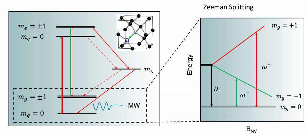
In recent years, the field of quantum sensing[1] has witnessed a revolutionary advancement with the emergence of nitrogen vacancy (NV)[2] centers as versatile and highly sensitive quantum probes. NV centers, found in diamond crystals, exhibit unique quantum properties that make them ideal candidates for a wide range of sensing applications.
The NV center consists of a nitrogen atom adjacent to a vacancy in the diamond lattice, along with two neighboring carbon atoms. It can be interrogated using optical techniques. When illuminated with green light, NV centers absorb photons and enter an excited state. Subsequently, they relax back to their ground state, emitting red fluorescence (c.f., Figure 1, box 1). The intensity and polarization of this fluorescence depend on the spin state of the NV center, which can be manipulated and read out using microwave and optical techniques. By precisely measuring changes in fluorescence, NV centers can be employed to sense and characterize various physical phenomena. On the other hand, as a single Q-bit, the electronic ground state of the NV center consists of a triplet spin configuration, i.e., m_s = 0, ±1. When no external magnetic field is applied, |-1> and |+1> energy levels are degenerated. However, when an external magnetic field is introduced, the energy levels experience a Zeeman splitting due to the interaction between the electron’s magnetic moment and the magnetic field. According to the Zeeman effect, the energy levels shift in energy, with the amount of splitting depending on the strength and direction of the magnetic field (c.f. Figure 1, box 2). By precisely measuring the energy splitting and phase differences between spin states, NV centers can be employed as ultra-sensitive sensors in diverse fields such as magnetometry, bio-imaging, quantum information processing.
Figure 1. NV center energy diagram and Zeeman splitting
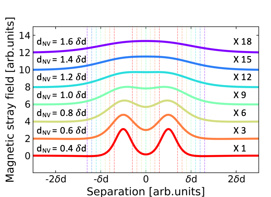
Although NV center offers unparalleled sensitivity in real space imaging, one of its limitations is the requirement for close proximity to the sample surface. This constraint poses challenges for imaging finer structures that require a lower stand-off distance. The spatial resolution of Scanning NV magnetometry (SNVM) depends on the sensor-to-sample distance dNV , as opposed to optical microscopy, whose resolvability is constrained by the diffraction limit, and other quantum sensing technique such as scanning superconducting quantum interference devices microscopy (or scanning SQUID microscopy) , whose resolvability is limited by the sensor size. Figure 2 shows the change of the z-component of magnetic stray field originating from two dipoles[3] separated by distance δd measured by NV at different dNV .
Figure 2. The SNVM measured z-component magnetic stray field above two dipoles separated by distance δd is modified by the sensor to sample distance dNV. At dNV = δd (light green curve), the FWHM of individual dipole equals to the separation between two maxims. Rainbow color sequence represents the different dNV , from 0.4 δd to 1.6 δd at each 0.2 δd interval. Stray field curves have been vertically offset for clarity and have been multiplied by a given factor to compensate for the weaker signal due to the large dNV .
It is evident that the peaks from two separated magnetic dipoles can be well resolved at small sensor-sample separation (dNV in the range of 0.4 to 0.8 of the dipoles separation δd). When dNV approximates δd, the distance between the two peaks equals the full width at half maximum (FWHM) of the stray field distribution curves. It makes distinguishing between two individual dipoles difficult. Beyond this point, the two magnetic dipoles can not be resolvable any longer. Analogous to the Rayleigh criterion, the spatial resolution in SNVM is defined as the smallest distance between NV and sources to be resolved.
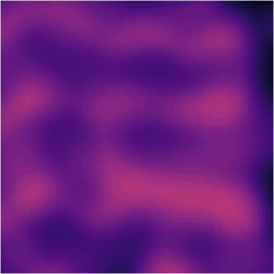
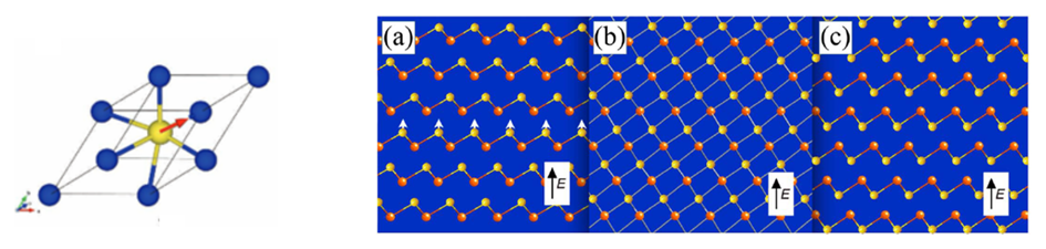
Figure 3. Images of a room temperature multiferroics bismuth ferrite (BiFeO3) by scanning NV magnetometry at different NV-to-sample distance. With decreasing standoff distance dNV, the spin cycloid (‘zig-zag’ shape patterns) can be well resolved.
Figure 3 illustrates the improved spatial resolution of SNVM through imaging the widely studied room temperature multiferroic material bismuth ferrite (BiFeO3)[4-6], known for its non-collinear antiferromagnetic spin cycloid that has garnered significant research interest in recent years. By shifting the NV center 21 nm closer to the surface of the BiFeO3 sample, the intricate ‘zig-zag’ pattern of the spin cycloid becomes clearly discernible.
In conclusion, the improved spatial resolution of scanning NV magnetometry represents a significant technological advancement with far-reaching implications across scientific disciplines. Through innovative techniques and methodologies, we have pushed the boundaries of spatial resolution, enabling nanoscale imaging of magnetic fields with unparalleled precision. As this field continues to evolve, scanning NV magnetometry promises to revolutionize our understanding of magnetism, quantum phenomena, and biological systems, paving the way for transformative discoveries and technological innovations.
[1] Degen, Christian L., Friedemann Reinhard, and Paola Cappellaro. “Quantum sensing.” Reviews of modern physics89.3 (2017): 035002.
[2] Degen, Christian L. “Scanning magnetic field microscope with a diamond single-spin sensor.” Applied Physics Letters 92.24 (2008).
[3] Lima, Eduardo A., and Benjamin P. Weiss. “Obtaining vector magnetic field maps from single‐component measurements of geological samples.” Journal of Geophysical Research: Solid Earth 114.B6 (2009).
[4] Gross, Isabell, et al. “Real-space imaging of non-collinear antiferromagnetic order with a single-spin magnetometer.” Nature 549.7671 (2017): 252-256.
[5] Haykal, A., et al. “Antiferromagnetic textures in BiFeO3 controlled by strain and electric field.” Nature communications11.1 (2020): 1704.
[6] Chauleau, J-Y., et al. “Electric and antiferromagnetic chiral textures at multiferroic domain walls.” Nature materials 19.4 (2020): 386-390.
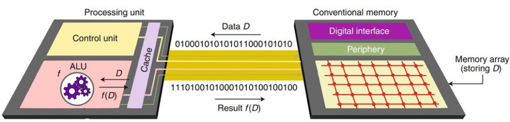
Memory Hierarchy – How does computer memory work ?
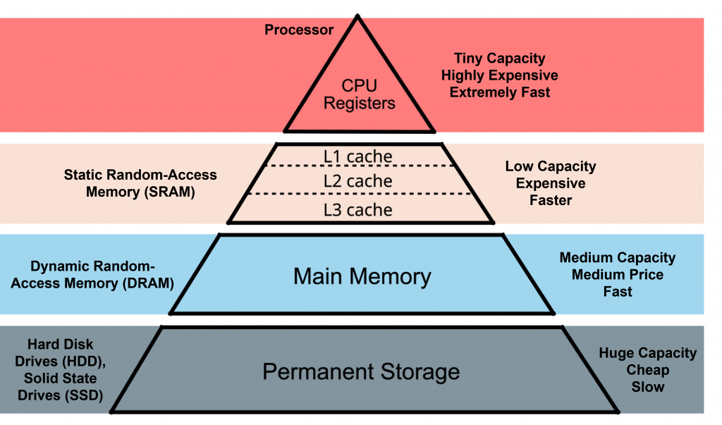
It’s 5pm on a Friday evening. I am done for the week. I save my half-completed article and prepare to leave. A fleeting thought says – “How is my file saved? How is data stored and accessed in a computer?” In this post, I try to answer these questions and understand how memory works in our computers with some examples. The file I saved is broken down into numerous bits or binary digits (0 or 1) and stored in memory units with each memory unit having either 0 or 1. Most computers are structured as a pyramid with the central processing unit (CPU) at the top as shown in figure 1. As we move downwards, we encounter short-term memory for frequently accessed tasks followed by long-term memory for permanent storage. While short-term memory is fast (5000-6000 megabytes per second) and has a smaller capacity (a few gigabytes) [1,2], long-term memory can be huge (a few terabytes) but is extremely slow (around 550 megabytes per second or less) [3]. Let’s take a look at the long-term or storage memories first.
Figure 1:The memory hierarchy or memory pyramid
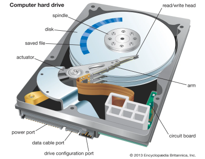
Two broad technologies exist for long-term storage – hard disk drive (HDD) and solid-state drive (SSD). HDD stores data in magnetic domains in layers of magnetic film deposited on a rotating disk as shown in figure 2. Writing and reading is achieved by a read/write head that can read the magnetic state of the domains. This technology was introduced by IBM in 1950s. HDDs are non-volatile and can retain data even after being powered off [3].
Figure 2:Internal structure and components of a hard disk drive. Information is stored in the magnetic state of the magnetic domains and is read or written by the read/write head.
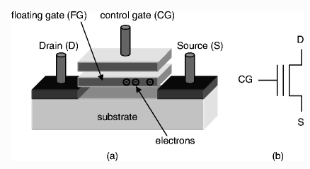
Figure 3:A floating gate transistor which is the basic building block of NAND Flash. A potential applied on the control gate results in transfer of charges from the transistor channel to the floating gate or vice-versa.
SSDs are based on a technology known as NAND Flash [4,5] developed by Fujio Masuoka at Toshiba in 1980s [6]. The basic building block of NAND flash is shown in figure 3. A potential difference between source and drain creates a channel of electron flow between them. Depending on the voltage applied at the control gate on top, some electrons are removed from or trapped in the floating gate. The presence or absence of the electrons results in a change in the resistance state of the device. Millions of such devices are arranged in a crossbar array to manufacture modern SSDs [3,7,8]. SSDs are 10 times faster than HDDs since they do not any mechanically moving parts. Although more expensive than HDDs, SSDs are used where high data transfer speeds and lower delays are desired. In case you haven’t already figured it out, modern thumb drives or flash drives are also based on the NAND flash technology. Most modern laptops and computers use SSDs for permanent storage whereas big data storage farms use a combination of HDDs and SSDs.
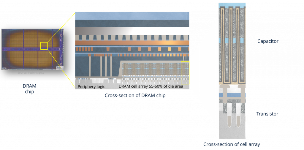
Figure 4:Cross-section of a DRAM chip and its cell array. Periphery logic is used to control the read, write and flow of information to/from the chip. Cross-section of the cell array shows the transistor and the capacitor of the 1T1C structure.
HDDs and SSDs are located at the bottom of the memory pyramid since they have huge memory capacity but slow access speeds. As we move up the pyramid, we come across dynamic random-access memory (DRAM) which is also popularly known as RAM. Also known as the main memory of the computer, DRAM stores the data of currently running programs. As the name random-access suggests, the data at any location in a DRAM can be accessed at any time. It was invented by Robert Dennard at IBM in the 1960s. The basic memory unit in a DRAM consists of a transistor and a capacitor in a 1T1C structure (shown in figure 4). Fully charged and completely empty capacitors denote 1 and 0 respectively. The source of the transistor is connected to the bitline (BL), the drain to the capacitor and the gate is connected to the wordline (WL). If we want to write a 1, the WL is opened, and the transistor is switched on. Electrical charges can now flow from the BL to the capacitor until it is fully charged. The transistor is then turned off and the charge in the capacitor is isolated. However, the charges are not perfectly isolated and leak out over time. The capacitive memory then must be re-written after a certain period [9]. Thousands of these 1T1C structures are arranged in arrays called banks. Multiple banks are combined to form a chip. Multiple parallelly working chips are combined to form the DRAM. DRAM has a capacity of a few gigabytes and access times in 10s of nanoseconds.
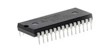
Figure 5:An SRAM chip
As we move further up in our memory pyramid, we come across cache memory. Cache memory stores frequently used instructions and data to improve computation time. Cache memory is implemented by a technology called static random-access memory (SRAM) (shown in figure 5). The memory unit of the SRAM is implemented by a combination of six transistors (6T). Since the operation of SRAM does not include the charging and discharging of a capacitor, it is faster than the DRAM. However, 6 transistors in a single memory unit in SRAM increase its cost and reduce the number of memory units that can be squeezed in a given area [10–12]. Cache memory is often referred to as “on-chip memory”.
What happens when I run a game, a software or just open a file?
Imagine I want to play the latest Assassin’s Creed on my computer. The game itself is installed in permanent storage (in the SSDs). When I run the game, the CPU sends around a lot of instructions to control the flow of data. The information is copied from the storage to main memory (to the DRAM). Remember the big “LOADING……” bar at the start? This transfer is necessary to reduce the latency while running the program and the reason behind minimum RAM requirements for all games and software. Depending on what part of the game you are currently playing, a part of the data is copied to the cache memory. Then, a part of that data on the cache is copied to the CPU registers and processed by the CPU. Now, imagine if the memory pyramid doesn’t exist and the CPU is forced to run the program directly from the permanent storage. Since the permanent storage is extremely slow compared to the cache memory, your agile assassin would be moving slower than a tortoise. Here are some videos (Video 1, Video 2) on YouTube that can help you understand more about how memory works in a computer.
How does spintronics come into the picture?
Multiple transfers of data make up most of the energy consumption of a computer. DRAM and SRAM are volatile memories which means once you turn off the power, all their data is lost and their memory needs to be re-written once they are turned on again. Also, as the size of transistors continues to decrease, the energy loss in terms of leakage current increases significantly. Current research is focused on replacing DRAM and SRAM with non-volatile technologies which can store data without the need for continuous power supply and have minimal leakage. One of the most promising solutions is to store data in magnets or magnetic devices. This has led to the development of magnetic random-access memories (MRAM). Spin transfer torque MRAM (STT-MRAM) products from Everspin technologies is already available in the market [13] and can compete with DRAM for certain applications. Meanwhile, spin-orbit torque MRAM (SOT-MRAM) [14,15] continues to garner interest from academia and industry and can potentially compete with SRAM in certain applications. Novel concepts for domain wall [16] and skyrmion-based [17] devices that can find their applications as CPU registers are also under development. While we continue to find solutions to improve our current computing scheme, there are plenty of emerging computing schemes that can overhaul the whole computing landscape. Check those out in previous posts (Maha’s blog, Marco’s blog, Paolo’s blog).
If you found this useful and/or would like to discuss further, don’t hesitate to contact me on LinkedIn.
References
[1] DDR5 | DRAM, https://semiconductor.samsung.com/dram/ddr/ddr5. [2] DDR5 SDRAM Datasheet and Parts Catalog, https://www.micron.com/products/dram/ddr5-sdram/part-catalog. [3] DC600M Enterprise SATA 3.0 SSD – 480GB – 7680GB – Kingston Technology, https://www.kingston.com/en/ssd/dc600m-data-center-solid-state-drive. [4] C. Monzio Compagnoni, A. Goda, A. S. Spinelli, P. Feeley, A. L. Lacaita, and A. Visconti, Reviewing the Evolution of the NAND Flash Technology, Proceedings of the IEEE 105, 1609 (2017). [5] NAND Flash Memory, https://www.micron.com/products/nand-flash. [6] F. Masuoka and H. Iizuka, Semiconductor Memory Device and Method for Manufacturing the Same, US4531203A (23 July 1985). [7] R. Micheloni, A. Marelli, and S. Commodaro, NAND Overview: From Memory to Systems, in Inside NAND Flash Memories, edited by R. Micheloni, L. Crippa, and A. Marelli (Springer Netherlands, Dordrecht, 2010), pp. 19–53. [8] SanDisk Ultra 3D NAND SSD 2.5" 250 GB – 4 TB SATA III Internal SSD, https://www.westerndigital.com/products/internal-drives/sandisk-ultra-3d-sata-iii-ssd.sku=SDSSDH3-500G-G26. [9] S. R. S. Raman, A Review on Non-Volatile and Volatile Emerging Memory Technologies, in Computer Memory and Data Storage (IntechOpen, 2024). [10] SRAMs | Renesas, https://www.renesas.com/us/en/products/memory-logic/srams [11] Synchronous SRAMs, https://www.alliancememory.com/products/synchronous-srams/ [12] A. Pavlov and M. Sachdev, editors , Introduction and Motivation, in CMOS SRAM Circuit Design and Parametric Test in Nano-Scaled Technologies: Process-Aware SRAM Design and Test (Springer Netherlands, Dordrecht, 2008), pp. 1–12. [13] Spin-Transfer Torque DDR Products | Everspin, https://www.everspin.com/spin-transfer-torque-ddr-products. [14] K. Garello et al., Manufacturable 300mm Platform Solution for Field-Free Switching SOT-MRAM, 2 (n.d.). [15] I. Mihai Miron, G. Gaudin, S. Auffret, B. Rodmacq, A. Schuhl, S. Pizzini, J. Vogel, and P. Gambardella, Current-Driven Spin Torque Induced by the Rashba Effect in a Ferromagnetic Metal Layer, Nature Mater 9, 3 (2010). [16] S. S. P. Parkin, M. Hayashi, and L. Thomas, Magnetic Domain-Wall Racetrack Memory, Science 320, 190 (2008). [17] R. Tomasello, E. Martinez, R. Zivieri, L. Torres, M. Carpentieri, and G. Finocchio, A Strategy for the Design of Skyrmion Racetrack Memories, Sci Rep 4, 1 (2014).
How to exploit magnets to make computers “better” in 21st century
The development and publication of artificial intelligences like OpenAI’s ChatGPT has attracted a lot of interest not only among scientists and (software) engineers but reaches deep into our diverse society. This technology provides obvious advantages but also causes undisputable issues and challenges. Next to ethical dilemmas, the tricky questions related to intellectual property and revolutionizing many jobs or making them obsolete, the immense energy consumption and corresponding emission of carbon dioxide required for training AI systems is widely discussed (Markovic et al., Nat. Rev. Phys 2, 2020).
Following Maha’s earlier blog post (“Neuromorphic Computing: A Brief Explanation” posted in December 2022, we recommend reading that one before delving into this second part) dealing with the von Neumann bottleneck and the basic functionalities of neurons and synapses, we will build up and try to exemplify in further detail, how magnetic systems can provide solutions to the imposed challenges. Therefore, the research field of spintronics tries to collaborate interdisciplenarily with researchers investigating the highly intriguing way the human brain works, and may perhaps also contribute to reducing the climate impact of this technological revolution which is on its way – for better or worse.
Conventional electronics uses „1“ and „0“ as elementary building blocks to save and compute information, also when emulating the potential in a neuron or the weight of a synapse. For instance, this implies that in order to have 32 different synaptic weight values accessible we need five elementary building blocks that can save one 1 or 0 to make up a number between 1 and 32 in the binary system. If instead we could find an alternative elementary building block, which has intrinsically 32 or more states available that is equally sized and may change its state at equal power and time scales, we could significantly improve our computing systems. Let us look at an example provided by spintronics for such an application:
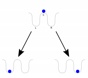
A so-called domain wall separates regions with opposing magnetizations (blue and red in the image below) in a magnetic material. Such a wall can be moved by electric currents into the direction of the electrons. This implies that by using charge currents, we can change the magnetic state of the material. Now, a device can be designed such that the position of the domain wall determines the measured resistance. This is achieved by so called magnetic tunnel junctions, which we are not going to describe in further details here. As the resistance of such a device can vary between many values, depending on the position of the domain wall, we can interpret this as a synaptic weight where not only 1 and 0 but many more values are possible. Ideally, the domain wall can stop anywhere within a material making numerous states available. In real devices, such domain walls will prefer to locate around imperfections in the crystal, such as impurities („wrong atom“) or vacancies („missing atoms“). By engineering a shape geometrically to provide „prefered locations“ for such domain walls, the number of accessible state can be controlled. In the work by Leonard et al. (Adv. Electron. Mater. 2022, 8, 2200563), notches at the boundary of the magnet provide such locations. Thereby, an artificial synapse is designed that can be driven and read out at low energies and fast.
Figure 1: Illustration of a notched domain wall track from Leonard et al., Adv. Electron. Mater. 2022, 8, 2200563. The blue area represents magnetization in the opposite direction as in the red area. The white vertical line is the domain wall, that can be moved by electrical currents and will get stabilized at one of the notches in equilibrium.
The location of a domain wall can also be used as a neuron potential such that this device could emulate a neuron. For this, a mechanism needs to be established that drives the wall back to one end in the absence of inputs, i.e. electric currents. One way to achieve this is by implementing a thickness gradient in the magnetic layer. Now, if a lot of currents accumulate within short enough times, the domain wall is driven across the device to the other end and the measured output value should be significantly changed only when it the wall reaches its (non-equilibrium) end. This can be engineered by the location of the read out sensors. In this way, simple magnetic devices can be used as both synapses and neurons.
Depending on the materials used in the fabrication process, the desired algorithms, energy footprint, data density and speed, various advantages and disadvantages emerge which need to be quantified and better understood and improved by spintronics researchers and engineers. It is being emphasized that conventional electronics is already performing on a high level and it poses quite a challenge to compete with that technology. Replacing conventional electronics entirely with a new system based on magnets or some other physical system, is very unlikely. However, such systems can fill gaps and perform particular subtasks in bigger computational problems, that conventional electronics are not highly suited for.
Another property of brain inspired networks that is hard to reproduce in conventional electronics is the high interconnectivity between different neuron layers. Some ten thousands of connecting synapses are typical in brains but very hard to implement in electronics.
Figure 2: Papp et al.,Nat Commun12, 6422 (2021) show how a magnetic system
Papp et al. (Nat Commun12, 6422, 2021) therefore demonstrate how to use a magnetic system in which the magnets are by default „talking to each other“ via their magnetic interaction and train the magnetic excitations of this system (so-called spin waves, which can be imagined similar to water waves) to tell apart different spoken vowels. Roughly, this can be imagined from the figure above in the following way: We have a plane of many little magnets (imagine a pool of water that experiences waves, that can be high or low just like the the magnetization can point upward or downward) represented by each of the three squares on top of each other. On the left the vowels are injected to the system as a high-frequency signal that excites the little magnets. If that sounds too crazy, think of a boat that can drive up and down on the left boundary of the pool at low, intermediate or high speed. The level of response (intensity of resulting water waves) is illustrated by the colors. The brighter the color the more the little magnets forward the information. The magnetic system can be trained by the implementation of some „fixed guiding magnets“ to redirect the incoming signals differently depending on what signal i.e., which vowel, was input. Perhaps you may think of buoys or obstacles in the water, that redirect the water waves. Thus, brighter color can be seen in the top, center or bottom part on the right side, where the signal can be read out again at one of the three white dots. Depending on which dot received the largest signal, the system recognized a different vowel (or a different speed of the boat).
This is an example (with a highly simplifying analogy of water waves) of how magnets can solve problems in a more elegant way by exploiting the wave nature of magnets than only implementing a lot of wires/connections with the conventional electronics.
As I am aware that some parts of this post may occur confusing and not intuitive right away, please do not hesistate to reach out to me, in case that you are interested to learn more of this emerging field of spintronics: marco.hoffmann@mat.ethz.ch .
How does a Scanning Tunnelling Microscope (STM) work?
How do microscopes work?
Each type of microscope uses different ways of obtaining information from the sample they are studying. Classical optical microscopes use light to probe the samples, this of course has its limitations, as light is just visible between certain wavelengths. This means that just objects slightly smaller than those wavelengths can be observed with them, setting the minimum observable distance with them at around 200 nm. Therefore, with this kind of microscopes we can study cells or other biological systems which are bigger than this distance, but we cannot obtain information of smaller things such as atoms.
But what if we want to observe these smaller things? One possible solution for that is using particles with smaller wavelengths as probes. This typically means using more massive particles, as the wavelength decreases when the mass increases. One of the easiest ways to do that is using electrons as waves, the microscopes that do that are called electron microscopes, and the most used ones are transmission electron microscopes (TEM) and scanning electron microscopes (SEM). With this kind of microscopy, it is possible to resolve objects down to around 15nm (High resolution TEMs (HRTEM) can reach 0.05 nm under very special conditions).
But there is another big family of microscopes. This is the scanning probe microscopy (SPM) family, to which STM belongs. All the techniques inside the SPM family are characterized for approaching the tip of the microscope to the sample to obtain information from it in different ways and then scan with it to form a complete image. Every technique inside this family uses different physical properties to work, and the property that STM uses is the quantum tunnelling effect (hence the name). With STM, features smaller than 0.1nm can be resolved horizontally, and 0.01nm features regarding depth. These values are especially useful as atoms have a typical size of around 0.3 nm, which means that STMs can achieve atomic resolution.
Figure 1.- Worm studied with SEM
The quantum tunnelling effect
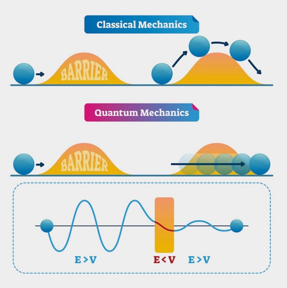
STMs use the quantum tunnelling effect as their principle of operation. This is a purely quantum mechanical effect that allows a particle to go through a potential energy barrier. If we make a comparison with the classical day by day world, it would be as if someone would go through a wall as a ghost, without interacting with it. This effect is related with the wave properties of the particles in the nanoscale, and the probability of it happening decreases the thicker the barrier is (the thicker the wall is for the ghost) and the bigger the particle is. What kind of particles are we talking about then? Well, some of the smallest particles that we humans know how to work with are electrons, so those will be the particles used in our STMs. And, what is a barrier for these electrons? A barrier is anything the electrons can’t go through. That can be an isolator such as plastic or wood, or in this case, the absence of anything, the vacuum.
If we apply a difference of potential in a wire, the electrons should be able to travel through it. But if we then cut the wire in the middle, the electrons will stop flowing from one side to the other. We will no longer have a current. The quantum tunnelling effect tell us that if we now put the two extremes of the wire really close (less than one atom of distance from one another), the quantum properties of the electrons will allow them to “jump” from one wire to the other quite often. The electrons will “tunnel” through the empty space and will reach the other cable, and the movement of electrons is a current, so then we will observe a current in our basic circuit even though it is not closed. As we know that the probability of tunnelling decreases when the barrier increases, if we separate our wires a little, the current will decrease, and if we put them closer it will increase. It will reach the maximum current when the wires touch, when we will observe the normal current that we had when the wire was not cut.
Figure 2.- Classical particles need enough energy to go over the barriers, quantum particles can go through the barriers instead.
So how does a STM work then?
Let’s imagine our theoretical circuit already cut in the middle. The only important things here are the wires and the gap in between them. The wires are made out of metal and the gap is made out of nothingness. Perfect. Now we want to see tiny things with this setup, so the first thing is choosing what we want to see; that’s the sample. The sample is going to be attached to one of the cut sides of the wire, which makes of it just the new end of the wire as it is also metallic. Then we take the other cut side and we sharpen it. We sharpen it the best we can until the very tip is just one atom thick; this is our tip. If we now approach the tip and the sample we will get the same thing that we got before with the two cut wires: some current going through due to the tunnelling effect when really close, but there is a difference, our tip is now one atom thick. This means that if we now move to the side we can observe the current in a different atom. We can keep moving the tip sideways keeping it at the same distance of the sample all the time (this means making sure we let the same current go through the vacuum), but sometimes the sample will have holes (so we will have to approach the tip) or mountains (so we will have to retract the tip). If we keep track of how do we have to move the tip to keep the current constant, we will get lines of the topography of the sample! If we stack several lines of the topography, this is, if we scan the surface of the sample, we will get complete three-dimensional images of the sample!
Of course, all the details about how to keep the wires so close without touching, how to move the tip sideways, how to read the currents, etc. are complex issues that require high level engineering to be solved, but those are not the things that explain how a STM works. Many other things have to be done to properly obtain images out of these microscopes, for example, due to the close distance between tip and sample, it is necessary to have damping systems in order to decouple the microscope from any kind of vibration that could crash the tip into the sample.
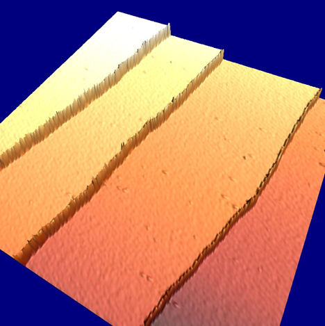
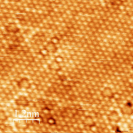
Figure 3.- Monoatomic Iridium step edges and terraces observed via STM. Size of the image is 300x300nm.
Figure 4.- Closer look to the Iridium surface showing individual Iridium atoms arranged in a hexagonal structure. Some defects can be seen in the sample.
References:
Figure 1: Philippe Crassous / FEI Company (www.fei.com)
The relation between magnets, symmetry and future computer technologies
Introduction, computers and information storage
I would like to anticipate that the present post is going through several different topics, and chances are that the reader might not be familiar with any of them. I hope anyway to be able to provide several inputs, so that maybe some of them might trigger the curiosity of the reader. The objective of this post is to make a connection between technology, and therefore objects which belong to our everyday experience; and some of the fundamental and fascinating concepts of physics, which enable the technology to work.
In the first part, I will talk about objects who possess some computing functions, focusing on information storage. In the second part, after a short explanation on magnetism, it is shown how information storage is made possible by the physical phenomenon known as symmetry breaking. In the end, I will talk about how broken symmetry systems can be also useful for novel computing technologies.
As we use any computing device, when we input any command, what is actually happening,, is an electrical charge flow. The device we are using consists of: a processor, that performs a modification on the information; and a memory, where the information, in form of a ‘0’ (zero) or ‘1’ (one) is stored. At any clock cycle, some information, is taken from the memory, the processor performs a mathematical operation on these information (sum, multiplication, etc…) and the result is stored in the memory. Any computer program, any app installed on the phone, no matter how complicated it might seem, is a sequence of these operations.
Although several ways can be employed to store temporarily an information coming from a computation stage, to later use it for the next one, our daily usage of electronic devices requires also that, once the power is turned off, the data is not deleted. This is the case for non-volatile memories, whose story begins when IBM sold the first Hard Disk Drive (HDD), in 1956.
In hard disk, the information (‘0’ or ‘1’), is stored in some materials, known as ferromagnets (called also magnets in a colloquial way). Magnetic materials have played an important role in information storage, even before HDD, for example in Vynil music recording. Today new memory concepts are being explored, like MRAM, that still makes use of magnetic materials.
Magnetism, ferromagnetic materials and symmetry breaking
The first thing coming to our mind when it comes to magnetism is the property of some materials, like iron, of attracting or repulsing each other. These materials are called ferromagnetic and are defined by the property of keeping their magnetization even though no magnetic field is applied. This definition opens, at least, the question of what magnetic field and magnetization are.
I’ll introduce magnetism with a high school example. Let’s consider two metallic wires through which an electrical current flows. Let’s imagine to control separately the two currents, being able to decide the intensity and direction of the flow.
The first thing we do is to apply the same current in the same direction and make the two wires approach each other. We will see that, as the two wires approach, they tend to repel each other. The more the distance decreases, the more the force exerted between the two intensifies. If the amount of current flowing increases, the force increases as well. If the direction of the current flowing in one of the two wires is changed, the force will have opposite sign, and the two wires will attract each other.
In physical terms we will say that a magnetic field is associated to the current flowing through the first wire, which results in a force exerted to the electrical charges in the second wire. Of course, the explanation works also the other way round, as the current in the second wire generates a magnetic field as well.
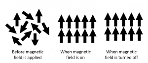
This phenomenon closely resembles the attraction and repulsion of magnetic materials, and in fact the root is the same. Magnetic field, in fact, is associated to the flow of an electrical current and, at the atomic level, magnetic materials are composed of microscopic spires of current, called magnetic moments. In ferromagnetic materials, as an external magnetic field is applied, the magnetic moments will tend to align to it and, if the magnetic field is turned off, they will (tend to) keep the same direction (cfr. Figure 1). The build-up of the magnetic field generated by these spires is known as magnetization. This is the property exploited in information storage, where the data is encoded in the magnetization direction of a permanent magnet.
Figure 1
If watched closely, the property of ferromagnetic materials that makes them useful is their order. In fact, in nature, sometimes, systems tend to spontaneously get ordered.
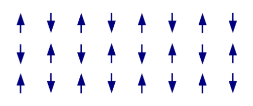
Ferromagnetism, in a material, occurs below a temperature known as Curie temperature. Let’s imagine to take a sample of Cobalt, above his Tc (around 1388°, but below its melting point, 1495°) and to cool it down. Cobalt is known to have an easy direction for the magnetization, therefore, as Tc is crossed, the magnetic moments will pass from a highly disordered (or symmetric) state, where each of them is randomly oriented, to a state where there is a favorite magnetization direction (broken symmetry). This is called spontaneous symmetry breaking and is a very broad natural phenomenon.
Figure 2
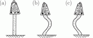
In physics, symmetry is the property of invariance upon a certain modification. For example, rotational symmetry is the property of anything that does not change upon rotation, and so on. In nature, it might happen that a system has the possibility to lower its energy by breaking some of its symmetry, hence choosing a well-defined state in place of the symmetric one. For example, a ball on top of a perfectly symmetric hill can lower its gravitational energy by choosing the direction of fall, thus breaking the rotational symmetry of the system “hill+ball” (cfr. Figure 2). Interestingly, it will be the slightest breath of wind to determine the direction of fall, and thus the final state of the system. Another analogous case is the Euler strut. As an increasing vertical force is applied to it, at some critical point, the strout bends, breaking again rotational symmetry (cfr. Figure 3).
Figure 3
Examples can go way further: any crystalline material (metals, e.g.) breaks translational symmetry; superfluids (if you don’t know what they are, look for them on YouTube and have fun) break a symmetry called “gauge”; moreover, according to astrophysicists, directly after the Big Bang, a symmetry breaking phenomenon has originated the growth of the universe.
Novel computing concepts
Now we are done with the first goal of the post, which was to connect a technology that is present in our daily use to one of the most fundamental and ubiquitous concepts of physics.
In the last part, I would like to run the path in the opposite direction, and connect broken symmetry systems some novel concepts of computing. Recently, the exponential improvement of computer performances has started to slow down and, at the same time, new concepts for computing have been proposed. Interestingly, broken symmetry systems play a role for many of them.
The first concept I am talking about is in-memory computing (IMC). As I described in the first section, in standard computers, the storage and the processing units are separated. The communication between them is known as a bottleneck, being the part that mostly slows down the operations. To overcome this, it has been suggested to change the architecture, and to have computation and storage units, that receive several inputs, perform operations between them and store the data. IMC is based on broken symmetry systems, like ferromagnets, but also ferroelectric (aligned electric dipoles), and phase change materials (change from amorphous to crystalline, breaking translational symmetry), and on building units to efficiently control the material order parameter (i.e. magnetization, polarization etc.).
The second interesting concept regards neuromorphic computing. The idea is to build a network of elements (neurons) connected by a variable weight (synapse). This network can perform algorithms specifically designed for artificial intelligence. The role of broken symmetry systems, here, is to have a continuous variation of the order parameter (e.g. rotation of magnetization or polarization) to be associated to the weight of the synapse.
With these two extremely quick mentions, I am concluding this post. I hope that, after reading it, there is some more curiosity on the topics treated, and some more awareness on the connection between science and technology.
An interview with Arturo Rodríguez (ESR12, UHAM) was recently published in the local newspaper of La Rioja, Arturo’s hometown. In the article, our ESR describes working with STM and life as a PhD student at University of Hamburg.
English translation below!
“I couldn’t resist writing my initials with twenty-nine atoms”
Arturo Rodríguez · In Hamburg, with the most powerful microscopes in the world
JAVIER ALBO
SANTO DOMINGO. The young man from Santo Domingo de la Calzada, Arturo Rodríguez Sota, is the beneficiary of an ITN Marie Curie scholarship in the European Union funded SPEAR (Spin-orbit materials, Emergent phenomena and related technologies training). He is studying for a PhD in Physics in Hamburg, for whose University he works.
What is your mission? My project is based on looking for skyrmions in the vicinity of superconductors, which are two very specific things that don’t get along very well. If I were to find them, it would be a great advance for the creation of quantum computers and other very promising technologies related to them, in addition to opening the door to exciting new physics, such as, perhaps, Majorana fermions. In a more general way, one could say that I work with scanning tunneling microscopes (STM) to study matter at the nanoscale. They are the most powerful microscopes in the world and allow us to observe individual atoms. They get their name from the principle on which they are based, a quantum effect called the Tunneling Effect, which allows electrons to overcome potential barriers as if they were ghosts walking through walls. The information obtained from this type of experiment enables the development of nanotechnology on which our phones and computers are based. Our group specializes in the study of the magnetic properties of these systems, for which we use a special microscope type (SP-STM), which, in addition to all of the above, it allows us to observe the magnetic moment or spin of the atoms.
What is it like working in your team? My group is very good, both scientifically and personally. I work surrounded by wonderful people like my supervisor, Dr. Kirsten von Bergmann, or those who have already become good friends as well as promising scientists Jonas Spethmann and Vishesh Saxena. Working with them is a combination of learning, enjoying and improving. We do science together and science is not knowing, to finally end up knowing. Working with them I have learned that the most beautiful thing someone can say is “I don’t know”, and then immediately search for the answer with all their heart. I’m happy.
What has surprised you the most to see or do on the other end of the microscope? Simply the fact of being able to see individual atoms already seems to me a feat worth mentioning. They only measure a fraction of a nanometer! One of the most beautiful things I have found were some atoms that naturally bunch together in groups of three due to an asymmetry. They look like little hearts! I usually say that I have discovered “the smallest hearts in the world”. Besides that, these microscopes not only allow you to see, but also to ‘touch’ and move individual atoms. As soon as I had the chance to work with them, I wasn’t able to resist writing my initials with only 29 atoms. It is something that will stay with me for the rest of my life.
Caption: Arturo, with the microscope he uses and his initials written with atoms.
Have you ever thought about why we can not perform brain tasks on our computers? Well of course I don’t mean a simple cat/dog recognition, or calculus (Computers have been specifically designed to do a very limited number of brain functions extremely well – even better than humans), but something bigger like analyzing new and unfamiliar situations.
To answer this question, let’s first see how conventional computers work:
Simply explained, there are two main units: a processing unit to process and analyze the data and a memory unit to store them. These two blocks are separated from each other and every time that a task must be done, the data should go back and forth between these two units. This architecture is known as Von Neumann architecture [1].
Fig1: Von Neumann architecture: in a conventional computing system, when an operation f is performed on data D, D has to be moved into a processing unit, leading to significant costs in latency and energy [2].
As you’ve already found out, there are two issues with this architecture that makes it almost impossible to do heavy tasks with:
Energy consumption, as the blocks are “separated” and lots of Joule heating can happen in between.
Not fast enough, due to the time required for the data to go back and forth.
This is also known as the Von Neumann bottleneck [3]. In other words, the architecture causes a limitation on the throughput, and this intensive data exchange is a problem. To find an alternative for it, it’s best to take a look at our brain and try to build something to emulate it, because not only is it the fastest computer available, but it is super energy efficient.
The brain is made up of a very dense network of interconnected neurons, which are responsible for all the data processing happening there. Each neuron has three parts: Soma (some call it neuron as well) which is the cell body and is responsible for the chemical processing of the neuron, Synapse which is like the memory unit and determines the strength of the connections to other neurons, and Axon which is like the wire connecting one neuron to the other.
Fig2: Neural networks in biology and computing [4].
Neurons communicate with voltage signals (spikes) generated by the ions and the chemicals inside our brains. There have been many models presented on how they work, but here will be discussed the simplest (and probably the most useful) one: The leaky integrate and fire model [5].
Fig3: leaky integrate and fire model, Incoming pulses excite the biological neuron; if the excitation reaches a threshold, the neuron fires an outcoming spike, and if not, it relaxes back to the resting potential [6].
As it was said earlier, neurons communicate with spikes which can change the potential of the soma. If a spike from a previous neuron arrives at a neuron after it, the potential of the soma increases. However, this is temporary, meaning that if no other spikes arrive afterward, the potential of the soma will reach the relaxed level again (leakage). On the other hand, if a train of spikes arrives at the neuron, they can accumulate (integrate) and if the potential reaches a threshold potential, the neuron itself will generate a spike (fire). After firing, the potential will again reach the relaxed level.
Apparently, the connections between all the neurons are not the same, and the differences are in the synapses. The form and combination of the synapses change in time depending on how active or inactive those two neurons were. The more they communicate, the stronger and better their connection, and this is called “synaptic plasticity”. (This is why learning something new is so hard because the connections between the neurons need time and practice to get better!). For more investigation into the fascinating world of the brain, this book is recommended: Neuronal Dynamics: From Single Neurons to Networks and Models of Cognition [7].
Now, it’s time to get back to the Von Neumann bottleneck. With inspiration from the brain, it can be seen that it’s better to place the memory unit in the vicinity, or even inside, the processing unit (just like the soma and the synapses which are really close), this way so much time and energy can be saved. It is also obvious that the processing units are better to be nonlinear as in the brain, and the memory unit should be able to be changed or manipulated to mimic the synaptic plasticity. We know how different parts should behave in order to have a computer to at least function like the brain, but the big question is: What hardwares should be used? What kind of devices act like a neuron, or a synapse? And even if we find them, are we able to place them close to each other to overcome the Von Neumann bottleneck?
These are the questions that Neuromorphic computing tries to answer. In other words, it is an attempt to build new hardware to be able to do computing like our brain. Some of the most promising candidates here are the spin-orbit devices as they are super-fast, energy-efficient, and more importantly, nonlinear [8][9]. I will talk about them and their major role in this field more in detail in the second part of my post soon!
1. Von Neumann, J. Papers of John von Neumann on computers and computer theory. United States: N. p., 1986. Web.
2. Sebastian, A., Le Gallo, M., Khaddam-Aljameh, R. et al. Memory devices and applications for in-memory computing. Nat. Nanotechnol. 15, 529–544 (2020).
3. John Backus. 1978. Can programming be liberated from the von Neumann style? a functional style and its algebra of programs. Commun. ACM 21, 8 (Aug. 1978), 613–641.
4. Bains, S. The business of building brains. Nat Electron 3, 348–351 (2020).
5. Brunel, N., van Rossum, M.C.W. Lapicque’s 1907 paper: from frogs to integrate-and-fire. Biol Cybern 97, 337–339 (2007).
6. Kurenkov, A., DuttaGupta, S., Zhang, C., Fukami, S., Horio, Y., Ohno, H., Artificial Neuron and Synapse Realized in an Antiferromagnet/Ferromagnet Heterostructure Using Dynamics of Spin–Orbit Torque Switching. Adv. Mater. 2019, 31, 1900636.
7. Gerstner, W., Kistler, W., Naud, R., & Paninski, L. (2014). Neuronal Dynamics: From Single Neurons to Networks and Models of Cognition. Cambridge: Cambridge University Press.
8. Grollier, J., Querlioz, D., Camsari, K.Y. et al. Neuromorphic spintronics. Nat Electron 3, 360–370 (2020).
9. Zahedinejad, M., Fulara, H., Khymyn, R. et al. Memristive control of mutual spin Hall nano-oscillator synchronization for neuromorphic computing. Nat. Mater. 21, 81–87 (2022).
Ferroelectrics are a category of material that in absence of an external applied voltage they still show a remanent polarization. The reason can be found in their atomic structure. For example the family of perovskites are ferroelectric material due to their specific crystal arrangement. Perovskite all share this similar ABX3 structure, where usually the X is oxygen and the A and B represent two different metals.
Fig.1 Phases of KNbO3 (potassium niobate) at different temperatures. It shows some structures where is possible to have a remanent polarization due to non-centro symmetry of the Niobium atom (in green) inside the cubic structure. When the Niobium atom is exactly at the center (in this case above 708 K) the material is not anymore ferroelectric [1].
One of most famous and studied is lead zirconate (PbZrxTi1-xO3) commonly called PZT. One of the biggest issues with this material is the toxicity due to the presence of the lead. For this reason, researchers focused on finding a material with similar characteristics. So many of them came out like barium titanate (BaTiO3), know as BTO or strontium titanate (SrTiO3) known as STO. In the picture here above another example of a lead-free perovskite material: potassium niobate (KNO3).
The remanent polarization properties is given by the presence of an atom inside this cubic-like structure that is not exactly at the center but slightly shifted. This non centro-symmetric structure give rise to a non-compensated positive charge of the body atom (Ti or Nb for example). The ferroelectric properties then are just given by the presence of the non-compensated charge when all the external voltages are removed. The temperature has an important role since for every material, for a given energy the structure tend to become a symmetric body centered cubic structure, hence there is a critical temperature after which the ferroelectric materials become paraelectrics. In this state they still react non-linearly to an external applied field but they do not show a remanent effect in absence of it.
Fig.2 Behaviour of a dielectric, a paraelectric and a ferroelectric material under an applied external electric field [2].
The polarization bistability for a zero external applied field is the key feature that makes ferroelectrics good candidates for memory applications. In recent year, many studies focused on integrating the ferroelectric materials in order to create new memories, more competitive from an energy computation point of view or overall faster writing and reading speed as FE-Fet [3], FE-RAM [4] or MESO [5] and FESO [6]. If for the first two the ferroelectric properties are aimed to improve the properties of already existing devices, like transistors or non-volatile random access memories; for the MESO and FESO case the aim is more ambitious. The idea is to develop a new logic based on spin controlled by ferrolectric non-volatility.
Recently, others materials showed to have ferroelectricity properties like Germanium telluride (GeTe), Indium arsenide (InAs) and many others. These materials show a simpler combination of only two atoms and that are not insulating like perovskites (sually they are metalic or semiconducting).
The bigger advantage is the possibility to pattern them in order to produce nanodevices, given by an higher durability when subjected to nanofabrication steps like etching. This one tend to destroy the crystal structure and hence the properties of the insulating perovskites . As a consequence, these new materials bring the ferroelectric-based devices a step closer to mass production and adoption.
If we take into account the case of germanium telluride, the ferroelectricity comes from the unusual bonds between germanium and tellurium layers. They tend to form a stronger bond with a neighbour layer with respect to the other forming a bilayer structure that is not symmetric (see pictures below). Similarly under an applied electric field the structure reorganize, causing the polarization to change sign (if the field is strong enough). It can be also seen as the germanium in the center of the cell moving along the larger diagonal of the deformed cubic cell (also called rhombohedral cell, left picture).
Fig. 3 Left: Cell structure of Germanium telluride (yellow Germanium, blue tellurium). Right: Switching mechanism: a) stable configuration of layer of Germanium (yellow dots) bonded to Tellurium ones (in red). b) when an electric field is applied, an unstable state appear where Germanium is bond to both top and bottom Tellurium atoms. c) Final state in which the Germanium atoms will be bond to the Tellurium atoms in the upper level with respect to the initial state [7]
So in a similar way to perovskites germanium telluride is know to show a remanent polarization at room temperature that can be controlled by an external applied electric field.
I hope you enjoyed this small talk on ferroelectrics, I will write in future a part 2 to explain the relation between ferroelectricity and spin-logic based devices. For further information you can email me at: salvatore.teresi@cea.fr
References
[1] P. Hirel et al., Phys. Rev. B 92 (2016) 214101.
[3] Stefan Ferdinand Müller (2016). Development of HfO2-Based Ferroelectric Memories for Future CMOS Technology Nodes. ISBN 9783739248943.
[4] Dudley A. Buck, “Ferroelectrics for Digital Information Storage and Switching.” Report R-212, MIT, June 1952.
[5] Manipatruni, S., Nikonov, D.E., Lin, CC. et al. Scalable energy-efficient magnetoelectric spin–orbit logic. Nature565, 35–42 (2019). https://doi.org/10.1038/s41586-018-0770-2
[6] Noël, P., Trier, F., Vicente Arche, L.M. et al. Non-volatile electric control of spin–charge conversion in a SrTiO3 Rashba system. Nature 580, 483–486 (2020). [7] A. V. Kolobov, D. J. Kim, A. Giussani, P. Fons, J. Tominaga, R. Calarco, and A. Gruverman, Ferroelectric switching in epitaxial GeTe films, APL Materials 2, 066101 (2014).
[7] A. V. Kolobov, D. J. Kim, A. Giussani, P. Fons, J. Tominaga, R. Calarco, and A. Gruverman, Ferroelectric switching in epitaxial GeTe films, APL Materials 2, 066101 (2014).
Hello readers! This first post is about antiferromagnets. I talk about the general concepts in antiferromagnetism and then later I dive into some interesting complex antiferromagnetic states at the atomic scale! I hope you have a good read! Please feel free to reach me out at my email for any further questions! (vsaxena@physnet.uni-hamburg.de)