Author: Niklas Kercher

Van der Waals Heterostructures: From Bulk Crystals to Devices

Materials science has made leaps in recent decades, particularly with the discovery and manipulation of two-dimensional (2D) materials—ultrathin sheets of atoms with unique electronic and magnetic properties. Everything began with the discovery of graphene in 2004, a single layer of carbon atoms with exceptional electrical and mechanical properties. Researchers in Manchester were able to separate a single layer of carbon from its bulk crystal using household sticky tape.

Building on this discovery, researchers began exploring other 2D materials, broadening the possibilities of material science. In the beginning, only a handful of materials were known and used for research. In addition to metallic graphene and insulating hexagonal boron nitride (hBN), more and more materials have been discovered, including magnetic materials, semimetals, and superconductors.

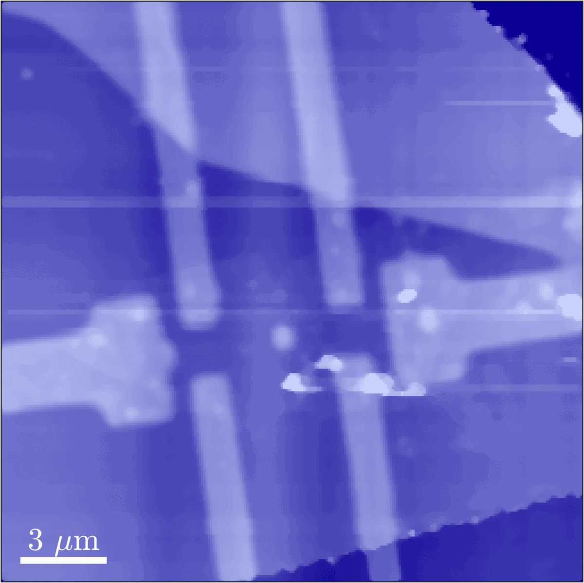
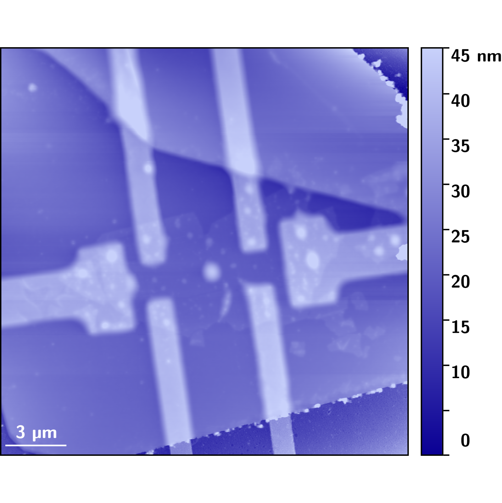
By stacking different 2D materials on top of each other, scientists can create van der Waals heterostructures. These engineered materials offer unprecedented control over electronic and optical properties, leading to significant advancements in electronics, quantum computing, and spintronics., named after the weak interlayer forces that hold them together. These structures allow researchers to tailor new materials with properties that do not exist in nature, leading to advancements in electronics, quantum computing, and spintronics. While the initial methods for creating artificial crystals were highly complex and had limited success, this changed with the introduction of the PDMS-PC dry stacking technique. A device that was created using this technique is shown in Fig. 1. The bulk material images were taken from the website of the Quantum Materials Lab of the University of Arkansas which provides a great overview of exfoliatable materials.

Fig. 1 Comparison of bulk crystals and artificial heterostructures created from exfoliated flakes of these materials.

Before constructing these heterostructures, researchers must first prepare the thin crystal sheets. Using adhesive tape, thin flakes of layered crystal are peeled from a bulk crystal. Basically, the thickness of the crystal pieces is halved with every iteration of opening and closing a piece of tape. Instead of the household scotch tape, researchers nowadays employ blue tape. This tape type of tape is usually used to cover example items to protect their surfaces and is used by researchers due to its low adhesive residues. The process is shown in Fig. 2. These flakes are then transferred on silicon wafers and inspected under an optical microscope to identify those with the right thickness and quality.

Fig. 2 a) Natural graphite flakes, and b), c) successive stages of the exfoliation process, illustrating the gradual reduction in thickness as layers are further separated.

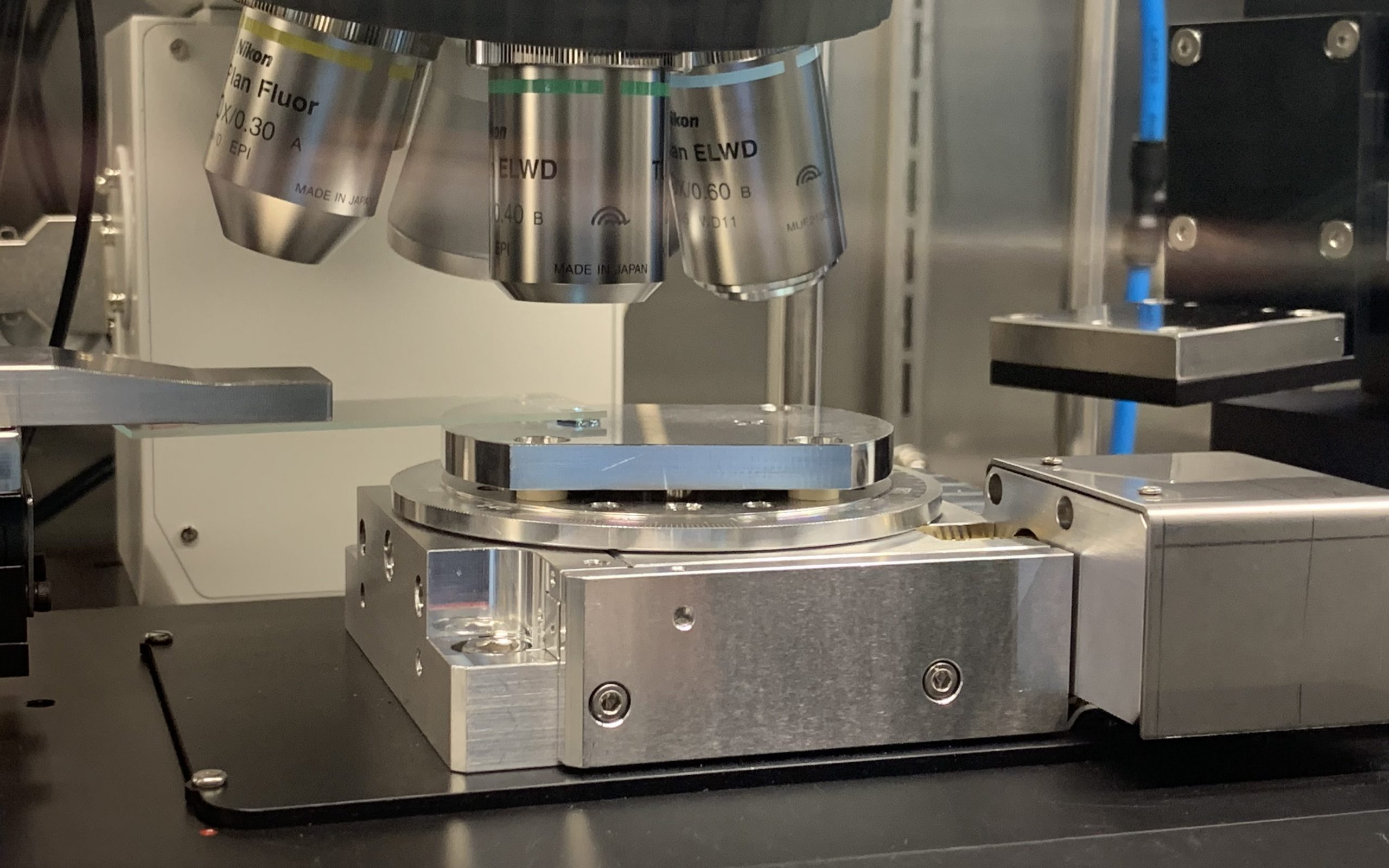
With the selected flakes in hand, researchers use the PDMS (polydimethylsiloxane)/PC (polycarbonate) Dry Transfer method to assemble artificial crystals layer by layer, ensuring precision and purity. As illustrated in Fig. 3, this process involves several key steps that allow for high control over layer alignment and minimal contamination.

Fig. 3 Step-by-step process of the dry transfer method using PDMS and PC: a) The PDMS-PC stamp is aligned over a selected flake. b) The flake is picked up by gently pressing the stamp while applying heat. c) The lifted flake is ready for stacking, and this process can be repeated to layer multiple flakes – usually, only the first flake requires heat. d) The stack is transferred to a different substrate. e) The flake is carefully aligned with pre-patterned electrical contacts and deposited at temperatures above 160°C. f) The PC layer is dissolved in chloroform, leaving a clean, high-quality van der Waals stack.

A PDMS stamp coated with a thin layer of PC is used to pick up an exfoliated 2D material. This stamp is then aligned over the target substrate under a microscope. By carefully controlling the temperature and pressure, the material is released onto the stack without contamination. The polycarbonate layer is later dissolved, leaving a clean heterostructure. This dry transfer method provides a high level of control over layer alignment and minimizes impurities, making it an essential tool for studying and engineering advanced 2D material-based devices. Following, the steps are described in more detail:

  1. Flake Selection and Alignment: A PDMS stamp coated with a thin layer of PC is first aligned over a selected 2D material flake using a microscope. This step ensures precise positioning of the flake for pickup.
  2. Flake Pickup: The stamp is gently pressed onto the flake while applying mild heat. This softens the PC layer, allowing the flake to adhere to it. Once lifted, the flake is securely attached to the stamp.
  3. Stacking Multiple Layers: The pickup process can be repeated to stack multiple flakes on top of each other. Typically, only the first flake requires heat; subsequent flakes attach through van der Waals forces alone.
  4. Substrate Transfer: After assembling the desired stack, the PDMS-PC stamp is moved to a different substrate, such as a silicon wafer or a pre-patterned chip with electrical contacts.
  5. Final Alignment and Deposition: The flake is carefully positioned over pre-fabricated electrical contacts and deposited at temperatures above 160°C, which ensures good adhesion and minimizes contamination.
  6. Polycarbonate Removal: The PC layer is dissolved using chloroform, leaving behind a clean, high-quality van der Waals heterostructure, ready for further experiments or device fabrication.

Ultimately, van der Waals heterostructures serve as a foundation for next-generation nanotechnology, enabling innovations in data storage, high-speed electronics, and beyond. From spintronic devices that store information using electron spin to high-speed, ultra-efficient transistors, these materials push the boundaries of what is possible. By refining fabrication techniques, researchers can fine-tune these structures to develop new quantum materials, flexible electronics, and energy-efficient computing devices. As our ability to design and manipulate materials at the atomic level continues to improve, van der Waals heterostructures will remain at the forefront of scientific and technological breakthroughs.

Presenting Scientific Content

In addition to conducting research, presenting research is a crucial part of a PhD student’s life. Whether in the form of posters or talks at conferences, presenting your research is as important as the results themselves. An engaging presentation increases the likelihood that your work will be appreciated and, more importantly, understood. The most important goal is to improve the accessibility of knowledge. In particular, intuitive graphics and diagrams can be used to convey content more effectively. That is why we invest a lot of time and effort in creating high-density graphics. Depending on the type of content, such as posters, presentations or papers, different standards are applied.

In the case of a poster, the aim is to attract the interest of passers-by. The content must be visually appealing to attract people casually passing by. Given the limited space, the content must be well condensed without visually overwhelming the viewer. This is where an unconventional design can score points and allow for more creative freedom.

The original plots on the left were transformed and merged using a vector graphics programme into the figure on the right, which was used in a poster I presented at ICM24 in Bologna.

When designing a presentation, you are not limited by space, but by time, which requires well thought-out storytelling. In the case of a presentation, the focus is on clarity to effectively convey knowledge to the audience, while at the same time being visually appealing to keep their attention. It is important that the slides support the presentation and are not the presentation itself.

This type of image is intended to provide a concise and easy-to-understand overview and timeline of the processes used to support the text version.

Figures for papers are very different, where information density needs to be maximised. Since the number of pages and figures is usually very limited, careful planning is required to decide what content needs to be presented. As figures are often made up of different sub-plots, the structure must be rigorous to ensure that the content is intuitively understandable and the relationships are clear. I want wo use an example from my Master thesis, where represented the process steps to fabricate the samples:

This type of image is intended to provide a concise and easy-to-understand overview and timeline of the processes used to support the text version.

Creating figures and schematics allows me to use my creative and graphic design skills, which is a nice balance to my working day. The process of translating complex data into clear and engaging visuals is both challenging and fulfilling. Creating these graphics allows me to combine scientific accuracy with an artistic touch, making the information more accessible. Whether I’m designing a poster, presentation or figure for a paper, I find satisfaction in the careful attention to detail required. This combination of creativity and science makes presenting research an enjoyable and meaningful part of my job.

My Second Secondment Journey: Back to the Roots

The transition from my home university in Zurich to my 10 weeks secondment at CIC nanoGUNE began with a long train journey on the TGV from Zurich to Hendaye, with a stopover in Paris. The next morning, I was warmly welcomed by the nanodevices group. Many faces were recognizable from my previous visit two years ago, yet, as is often the case, there was a noticeable turnover as well. In addition to scientific discussions, many members of the group shared their insights into local life. The food recommendations, especially the cheesecake, were much appreciated.

During my stay, I took the opportunity to explore Donostia and the surrounding areas, including a visit to Vitoria-Gasteiz. This city, known for its well-preserved medieval architecture, provided a pleasant escape and a chance to experience the local culture.

View of La Concha beach, situated on the Donostia coastline, and fireworks displayed during Semana Grande.

My academic journey took me to several places. The first was the European School on Magnetism (ESM) in Miraflores de la Sierra, where I met many new people in the field and learned a lot about the basics of magnetism, simulation, and characterisation techniques. As I had to travel via Madrid, I used the weekend to explore the city and meet members of the Zurich group and other ESRs who were in town for the JEMS conference.

Mixed impressions from Madrid and Segovia.

Later I went to Halle for the ESR training, where we covered the basics of topology and also had a soft skills session. A memorable part of this trip was when my train from Paris was cancelled, causing a 3-hour delay that would have left me stranded in Erfurt for the night. Fortunately, Deutsche Bahn arranged a taxi for the last 100 km, turning my trip into a 19-hour adventure.

Now that my time at nanoGUNE is coming to an end, with my departure scheduled for Thursday the 19th, I am preparing to say goodbye to the new friends and colleagues I have made here. As a thank you for their help and support, I plan to bake a Basque cheesecake for everyone. The thought of returning to Zurich brings a mixture of emotions. I am looking forward to continuing my research at my home university, but I will certainly miss the people and experiences I had during this secondment.

My attempts to bake a fluffy Basque cheesecake with flavours of caramelised sugar and vanilla.

The trip was full of learning, both academically and culturally. Additionally, the secondment reminded me of the beginnings of my PhD, as it was here that I received an introduction to the finesse of glovebox stacking. I have gained a deeper understanding of my area of research, particularly in flake formation and transport measurements. The many interactions, both formal and informal, have enriched my PhD experience, and I am eager to apply the new knowledge and skills as I continue my research back in Zurich.

The satisfaction of repairing

An important part of PhD life is maintaining devices you are supervising. For example, besides other devices, I am responsible for our atomic force microscopy (AFM). This type of microscope uses a fine tip to characterize a surface with up to picometre precision. In comparison to scanning tunnelling microscopy, the feedback is generated from changes in cantilever properties rather from a tunnelling current. In my group, mainly use the so-called tapping mode, where the cantilever is resonantly driven and the change of the resulting amplitude due to the close by sample is used as feedback. This way of imaging a surface is advantageous since it reduces the force exerted on the sample.

Image of the unmounted AFM body with view on the optics. The scanner was removed before and is shown on the right. The problem was a loose connection between the two components.

Recently, our roughly ten-year-old machine was experiencing some troubles. Occasionally, the scanner was not detected any more when the scanning unit was moved. It is designed that way, that the scanner needs to be pulled out to exchange the cantilever with the tip. A semi-flexible multilayered PCB cable connects the scanning with the mainboard of the AFM. The dynamic-cyclic loading degraded this cable over time. To confirm our first assumption, I took the AFM apart, removed the cable and checked if the pins on both ends are all still connected. As expected, depending on the bending, several pins are shortcut and several lose their connection.

Cable connecting the AFM mainboard and the scanning unit.

After reassembling the entire unit and making a few minor adjustments, the AFM will work fine until the replacement part arrives. Finding these temporary solutions is an important lesson during the doctoral studies, as it enables a variety of technical problems to be solved, whether just as a bridging solution or a complete repair. For my research, atomic force microscopes are a useful tool to measure the thicknesses of exfoliated crystals, to clean surfaces of flakes or flattening heterostacks as shown in the following images.

Fabricating Sunglasses with High School Students

In the scope of ETH outreach week, my colleague Patrick and I showed high school students how thermal evaporation works. The idea of this week is to give high school students from Switzerland and abroad can get hands-on insights on different study programs, in our case materials science. We first introduced them to the general basics of thin films in general, absorption and different principles of film deposition.

In our case, a thermal evaporator was used to vaporise the source materials. Following, a sketch of the device is shown. It is an easy principle: in an evacuated volume, the material is heated inside a crucible until atoms and small cluster are evaporated. The vacuum is needed to prevent contamination of the film and to ensure the particles reach the substrate. At the substrate, the atoms and clusters condensate on the surface and form a film, just as any other surface inside the chamber.

Sketch of a typical thermal evaporator design

The students were allowed to carry out all steps by themselves under supervision. Firstly, the lab safety glasses had to be prepared and cleaned well. Then, they were placed inside the chamber, which was evacuated next. Now, the source materials were melted by resistive heating, while slowly increasing the power the evaporation rate was observed via an oscillating quartz crystal. After the desired rate was reached, the shutters were opened and the Poly(methyl methacrylate) (PMMA) glasses were coated.

The students were able to decide from different materials, where aluminium and copper have been the most common choices. Some tried some more interesting ideas, like making a bronze alloy from copper and tin. As explained in our introduction, absorption rates vary among the used materials. For example, 100 nm thick aluminium films will completely reflect the light while copper of the same thickness is still quite transparent.

PMMA glasses coated with a 120 nm thick bronze film.

Especially for sunglasses, it is important to have UV filters to protect the eyes. We made sure that materials we evaporated block most of UV light (below 350 nm wavelength) to have safe sunglasses. Anyway, since we did not deposit a sealing layer, our films are not scratch resistant. Therefore, our sunglasses are more meant to be a nice souvenir from their week at ETH Zürich.

Getting connected

In the last two weeks, thanks to an early part secondment, I had the opportunity to get to know many different preparation and exfoliation possibilities at CIC nanoGUNE. Besides the many scientific experiences, I came into contact with many friendly and helpful scientists and was able to enjoy the time there, also because of the good weather. Besides Marco, who works with me in Zurich, I also got to know two other ESRs personally here, Mayank and Eoin. Fortunately, my time in San Sebastián/Donostia coincided exactly with a statistically significant accumulation of birthdays, so I got to enjoy freshly baked cake at work surprisingly often.

The view over one of the beaches of San Sebastián/Donostia towards the city center.

I spent most of my time at the glove box exfoliating various non-stable materials and building stacks with the stamping system. In the picture you can see the transfer process, where the flakes are transferred to a substrate using polydimethylsiloxane (PDMS). With this technique, precisely aligned complex hetero structures can be produced successively.

Stamping process mid stamping. The exfoliated flakes are on the PDMS which is on the bottom side of the glass slide.

Back in Zurich, I will continue the exfoliation of van-der-Waals crystals of different materials. The new knowledge I gained at CIC nanoGUNE and especially the personal tips on the exfoliation for specific materials will help me to fabricate different types of samples in the near future, either in a controlled environment or under ambient conditions.

Finally, I can only thank you for the wonderful time and send my greetings to Spain.

Diseño y desarrollo web Triplevdoble